News: LEDs
5 May 2022
UV-C LEDs with external quantum efficiency up to 8%
Researchers in Japan have used ‘face-to-face’ annealed (FFA) sputtered AlN (Sp-AlN) templates on sapphire to fabricate 263nm ultraviolet-C (UV-C) light-emitting diodes (LEDs) with state-of-the-art external quantum efficiency (EQE) [Kenjiro Uesugi et al, Appl. Phys. Express, v15, p055501, 2022].
The team from Mie University, Osaka University and University of Tokyo comments: “To the best of our knowledge, the developed UV-C LED has the highest EQE at a wavelength of approximately 265nm, even considering the state-of-the-art devices fabricated on sapphire substrates and free-standing AlN substrates.”
UV-C LEDs are sought to replace bulky, fragile and hazardous mercury lamps used for sterilization and virus inactivation, needing wavelengths shorter than 300nm. Presently, UV-C LEDs have low EQEs of less than 10%. The reported LEDs achieved EQEs up to 8% when the devices were suitably packaged and encapsulated.
The team has previously used its FFA Sp-AlN growth technique to reduce threading dislocation densities (TDDs) by an order of magnitude to 4x10⁷/cm2.
The Sp-AlN was deposited on sapphire substrate with a 0.2° off-angle in the m-direction. Two samples were grown at 700 and 750°C, respectively.
The wafers were subject FFA at 1600-1700°C for 36 hours. The FFA arrangement involves placing two wafers with the two AlN surfaces in contact ‘face-to-face’, avoiding thermal decomposition of the AlN at such high temperature in nitrogen at atmospheric pressure.
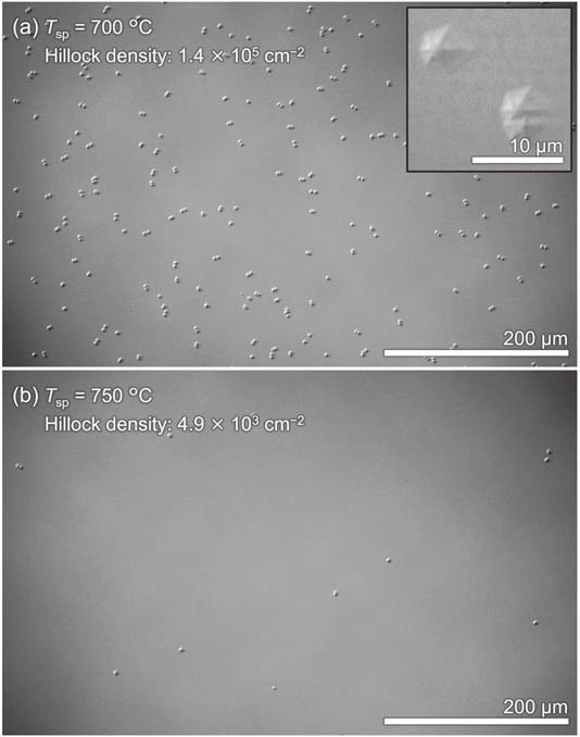
The resulting FFA Sp-AlN layer was 600nm thick. This was followed by metal-organic vapor phase epitaxy (MOVPE) of 200nm AlN and 300nm unintentionally doped Al0.7Ga0.3N. Life being what it is, the reduced threading dislocation density of the underlying AlN leads to increased fractions of screw- and mixed-type dislocations that present as “excessively large” hillock structures on the wafer surface (Figure 1).

Figure 1: Nomarski microscopy images of 300nm-thick Al0.7 Ga0.3N films grown on FFA Sp-AlN fabricated at sputter-deposition temperatures of (a) 700 and (b) 750°C. Inset: magnified image of typical hillock structures.
The hillock density was affected by the sputter temperature: 1.4x10⁵/cm2 and 4.9x10³/cm2 on AlN sputtered at 700 and 750°C, respectively. Clearly, the higher sputtering temperature is preferred. Previous FFA Sp-AlN grown at 600°C resulted in an even higher hillock density of ~106/cm2.
The researchers comment: “The occurrence of lower screw- and mixed-type FFA Sp-AlN dislocation densities at higher deposition temperatures can be attributed to the improvement in the c-axis orientational ordering of the AlN film in the as-sputtered state.”
Working toward LED structures, the researchers then grew 1μm silicon-doped (:Si) Al0.75Ga0.25N on FFA Sp-AlN by MOVPE. The researchers studied the effects of MOVPE growth temperature, rate, and ammonia/hydrogen (NH3/H2) partial pressures on the AlGaN:Si surface morphology. To maintain the Al content of the layer at 75%, the researchers also varied the trimethyl-Al/Ga precursor supply to compensate.
The study showed that the interest of low hillock density was achieved through high temperature (1100°C) and low growth rate (0.5μm/h), along with high NH3 partial pressure (10kPa). The effect of H2 partial pressure was insignificant. The optimized conditions reduce the difference in growth rates between the regions near and far from the screw dislocations.
The researchers comment: “Notably, the hillock density was independent of the MOVPE growth conditions for AlGaN, as it was determined by the density of the screw- and mixed-type dislocations in the FFA Sp-AlN template.”
The condition for reducing hillocks had the unfortunate effect of meandering step growth and pit formation. This was tackled with a 1050°C low-temperature 100nm AlGaN:Si interlayer before growing the UV-C LED structure.

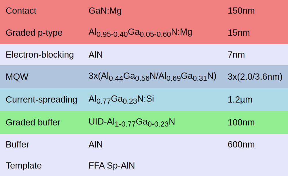
Figure 2: MOVPE layer sequence.
The template for the UV-C material was FFA Sp-AlN sputtered at 750°C and annealed for 51 hours at 1600-1680°C. The MOVPE layer sequence (Figure 2) included a multiple quantum well (MQW) consisting of three well/barrier pairs grown at 1050°C. The MQW was given a low silicon doping concentration of 3-5x10¹⁷/cm3, designed to reduce non-radiative recombination center density.
The 1.2μm n-type, silicon-doped current-spreading layer was mostly grown at 1150°C, except for the last 100nm grown at 1050°C.
X-ray analysis of the material suggested a hillock density of 7.2x10³/cm2. The researchers comment: “These values are the state-of-the-art low TDDs among the Al(Ga)N grown on sapphire substrates.”
LEDs were fabricated with nickel/gold p- and titanium/aluminium/nickel/gold n-electrodes. The sapphire substrate was thinned and polished to 150μm. The 400μmx300μm dies were singulated through laser scribing.
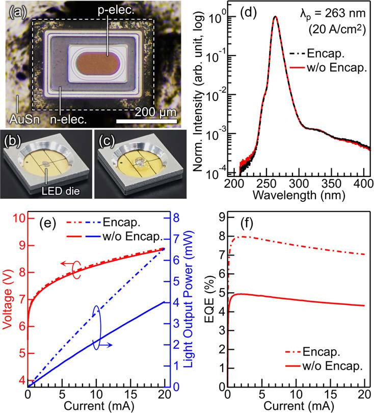
The chips were packaged flip-chip mounted on a 6.8mmx6.8mm2 sized AlN-based container-type ceramic package with gold-tin eutectic bonding and Al reflector (Figure 3). Some of the devices were encapsulated in UV-transparent silicone resin composed of poly(dimethylsiloxane) and poly(diethoxy-siloxane).

Figure 3: (a) Optical microscope image of as-mounted UV-C LED bare die in ceramic package. Dashed rectangle: edge of die. Photographs of packaged UV-C LEDs: (b) without and (c) with encapsulation. (d) Electroluminescence spectra. (e) Current-voltage-light output power characteristics, and (f) EQE results.
The peak wavelength of the emitted UV-C radiation was 263nm. Without encapsulation the external quantum efficiency reached 4.9% at 2.0mA injection current. Encapsulation increased the peak EQE to 8.0% at 2.9mA. The corresponding output powers at 20mA were 4.0 and 6.6mW, respectively. The researchers estimate the light extraction efficiency enhancement from encapsulation at 1.6x.
The high EQEs are attributed to improved internal quantum efficiency and, possibly, carrier injection efficiency. “The uniform thickness and AlN-molar fraction of the MQWs, AlN-EBL, and p-type AlGaN:Mg are attributable to the suppressed undesirable current crowding and overflow,” the team writes.
UV-C LEDs AlN templates Sapphire MOVPE
https://doi.org/10.1038/s41377-022-00753-4
The author Mike Cooke is a freelance technology journalist who has worked in the semiconductor and advanced technology sectors since 1997.


