News: Microelectronics
9 June 2022
Gallium oxide beats silicon power limit
Researchers based in the USA claim the first more than 4kV-capable β-Ga2O3 lateral metal–semiconductor field-effect transistors (MESFETs) surpassing the theoretical unipolar figures of merit (FOMs) for silicon-based devices [Arkka Bhattacharyya et al, Appl. Phys. Express, v15, p061001, 2022].
The team from University of Utah, University at Buffalo, Agnitron Technology Inc and University of California Santa Barbara (UCSB) also say that, to date, the devices show the highest maximum drain current (IDMAX) and lowest on-resistance (RON) simultaneously for any β-Ga2O3 with breakdown voltage (VBR) more than 4kV.
The 4.6-4.9eV ultra-wide bandgap of β-Ga2O3 implies high breakdown capabilities with potential for power-efficient next-generation high-voltage power devices. Breakdown voltages up to 8kV have been achieved, but practical devices also need low resistance for power efficiency.
A 230nm layer of β-Ga2O3 was grown on an iron-doped bulk substrate oriented as (010). The researchers used Agnitron’s Agilis 700 metal-organic vapor phase epitaxy (MOVPE) equipment with triethyl-gallium and oxygen precursors. Silane (SiH4) was the source for n-type silicon doping.

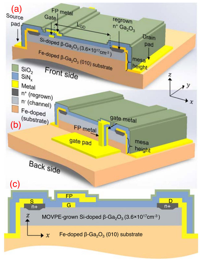
Figure 1: (a) 3D cross-section schematic of β-Ga2O3 MESFET showing FP design. (b) Gate FP metal electrically connected to gate pad outside mesa (inset: coordinate planes/axes) and (c) 2D cross-section schematic along x–z plane.
The mesa and recessed contact regions were fabricated using sulfur hexafluoride (SF6)/argon inductively coupled plasma reactive ion etch (ICP-RIE) – see Figure 1. The mesa height was 500nm, meaning that the etch continued into the substrate. The ohmic contact region consisted of heavily doped n+-β-Ga2O3 regrown in the recessed region.
The MESFET consisted of annealed titanium/gold/nickel ohmic source/drain contacts and a nickel/gold/nickel Schottky gate.
The titanium/gold/nickel gate field plate (FP) was insulated from the gate metal with 170nm of plasma-enhanced chemical vapor deposition (PECVD) silicon nitride (SiNx). The electrical connection between the gate and FP was made away from the device mesa. The FP fabrication was designed to avoid plasma-related damage in the active region.
The device mesa was finally passivated with a combination of 50nm silicon nitride and 50nm silicon dioxide. The gate length of the devices was 2.4μm, and the gate-source spacing 1μm.
Hall measurements gave a channel charge carrier density and mobility of 5.7x1012cm2 and 95cm2/V-s, respectively. The corresponding sheet resistance was 11.7kΩ/square.
The maximum on-current in devices with 34.5μm gate-drain distance (LGD) and 3.2μm FP was 56mA/mm at 2V gate potential. The on-resistance was 385Ω-mm. The device pinched-off sharply with the gate at -13V. The on/off current ratio was more than 108. The maximum transconductance was 6.2mS/mm, and the sub-threshold swing 186mV/decade.
The breakdown characteristics were explored with the devices submerged in FC-40 Fluorinert dielectric liquid. The breakdown voltage, with the device off at -20V gate potential, occurred with a drain-gate potential difference of 4415V. This naturally increased with 44.5μm LGD (3.5μm FP) to 4567V. Before the catastrophic breakdown the leakage varied in the range 10-100nA/mm.
The researchers attribute the improved breakdown performance on steps taken to minimize reverse leakage. The team comments: “The long HF substrate cleaning before the epilayer growth helped in suppressing the parasitic channel at the epilayer/substrate interface that is believed to come from residual silicon impurities from the substrate polishing or ambient exposure.” They also believe that the mesa etching deep into the substrate eliminates fringing leakage paths around the device mesa.
Devices with LGD less than 10μm demonstrated average breakdown fields (VBR/LGD) around 2.5MV/cm. Above 10μm LGD the VBR tended to saturate around 4.5kV.
On the basis of simulations, the researchers suggest that below 10μm LGD the field profile was of a punchthrough form with non-zero field at the drain contact at breakdown. Longer LGD resulted in a non-punchthrough field up to breakdown.
The simulations also raised concerns of the peak field occurring at the FP edge in the silicon nitride layer: “Dielectric leakage/breakdown could also be limiting the VBR and causing the saturation in VBR.” The team suggests that the dielectric performance would be improved by using materials with a high product of relative DC dielectric permittivity (ε) and critical electric field for breakdown.
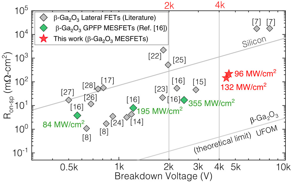
The VBR2/Ron,sp power figure of merit (PFOM) reached 132MW/cm2 for 34.5μm LGD. The specific on-resistance was normalized according to LGD and the transfer lengths of the source/drain contacts (0.6μm each). The longer 44.5μm LGD resulted in a lower 96MW/cm2 PFOM.

Figure 2: Differential Ron,sp-VBR benchmark plot of latest β-Ga2O3 MESFET with literature reports. Green data represent previous work of the team.
Commenting on benchmarking against other reports (Figure 2), the researchers write: “It can be seen that the devices reported here are the first >4kV-class β-Ga2O3 FET devices to surpass the theoretical unipolar FOM of silicon. Furthermore, our reported Ron,sp are the lowest for any β-Ga2O3 FET exceeding a breakdown voltage of 4kV.”
https://doi.org/10.35848/1882-0786/ac6729
The author Mike Cooke is a freelance technology journalist who has worked in the semiconductor and advanced technology sectors since 1997.


