News: Microelectronics
14 January 2022
Ohmic contacts on lightly doped p-GaN
Nagoya University in Japan reports improved Ohmic behavior for contacts on p-type gallium nitride (p-GaN) through using an annealed and treated magnesium layer [Shun Lu et al, Appl. Phys. Lett., v119, p242104, 2021]. The team comments: “Compared with other conventional methods such as continuous growing or regrowth, our process requires a lower temperature and pressure and can achieve a localized contact layer easily without any etching-induced damage.”
The researchers see benefits for a range of power electronics applications using components such as metal-oxide-semiconductor field-effect transistors (MOSFETs) or heterojunction bipolar transistors (HBTs), where low-resistance Ohmic contacts are essential for effective operation. GaN is favored for power electronics due to high breakdown electrical field, high saturated electron velocity, and high electron mobility. Good contacts with n-GaN are relatively easy to achieve with titanium and gold.
For p-GaN, the most common metal combination for contacts is nickel/gold, which forms a p-nickel oxide layer, but there is still a thin Schottky barrier through which carriers have to tunnel, reducing Ohmic characteristics. Most device structures add a heavily doped p+-GaN layer to improve Ohmic behavior.
In fact, the Nagoya technique allows contacts on lightly doped p-GaN to have better Ohmic behavior than the p+-GaN samples.
The researchers used a 4-step cleaning process to prepare a p-GaN surface before application of the Mg. The cleaning removed surface oxides, metal ions, and particle contamination. This was followed by 700°C annealing in nitrogen to activate the p-GaN layer.
The Mg contact layer was deposited using radio frequency magnetron sputtering with lift-off patterning. This was followed by 800°C annealing in nitrogen and 15 minute treatments with boiling aqua regia and then hydrofluoric acid. The researchers see the annealing and acid washing as key steps towards the annealed Mg contact layer.
The annealing increased the Mg layer thickness to 80nm. The annealed layer had a rough brown surface, having lost its “surface metal luster”. The acid washing reduced the layer to 20-40nm thickness. “We found that 15min is sufficient for removing the entire resistor-like layer,” the team writes.
The remaining Mg contact layer was found to be non-reactive with acid. Composition studies using scanning transmission electron microscope (STEM) energy-dispersive x-ray analysis suggested the Mg contact became a (Mg3N2)1-x(GaN)x alloy. The presence of Ga stabilized the Mg3N2, which on its own is very unstable in air.
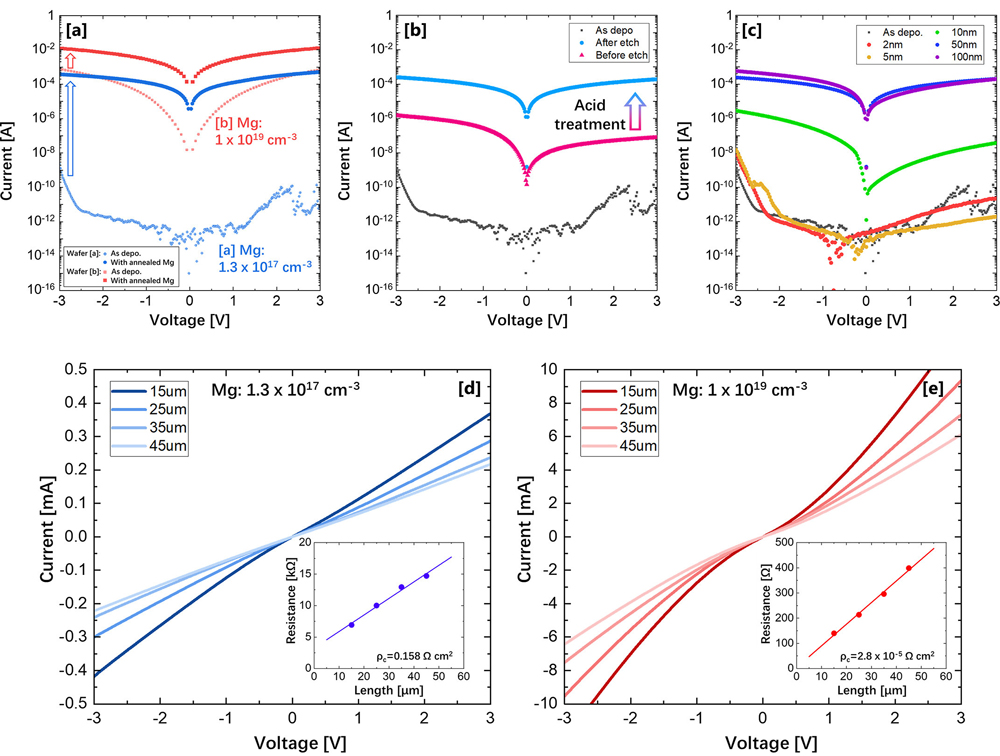
The effects of the separate steps were seen in electrical characterization (Figure 1). Without the Mg contact layer, the contact of a bare p-GaN layer, doped with 1.3x10¹⁷/cm3 Mg, on GaN/sapphire template with the electrodes was almost insulating. The annealed Mg contact increased current flow by a factor of order 105. The improvement with the thickness of the deposited Mg contact layer saturated at around 50nm.

Figure 1: (a) Typical current–voltage characteristics with and without annealed Mg layer. (b) Effect of aqua regia/HF treatment after annealing. (c) Effect of deposited Mg layer thickness on current–voltage characteristics. Current–voltage and resistance-distance dependence on p-GaN with (d) low and (e) high Mg concentrations as determined by CTLM.
A second sample on GaN substrate with 1019/cm3 Mg concentration p-GaN showed a lesser increase in current flow, an order of magnitude at high bias, but greater at low bias, improving linearity. The acid wash also improved the linearity of the 1.3x10¹⁷/cm3 Mg p-GaN sample, and increased the current flow from just annealing.
Circle transmission line measurement (CTLM) was carried out with annealed 20/150nm nickel/gold electrodes. The CTLM on the various contacts showed close to linear behavior with the 50nm layer on both samples, especially with low-Mg-concentration p-GaN.
The researchers estimated the specific Ohmic contact resistance at 0.158Ω-cm2 for the contact on 1.3x10¹⁷/cm3 Mg concentration p-GaN at -2.5V bias. The contact resistance on 1019/cm3 GaN:Mg was 2.8x10⁻⁵Ω-cm2 (-5V bias), reduced from 1.2x10⁻²Ω-cm2 for a normal nickel/gold electrode on p-GaN without Mg layer.
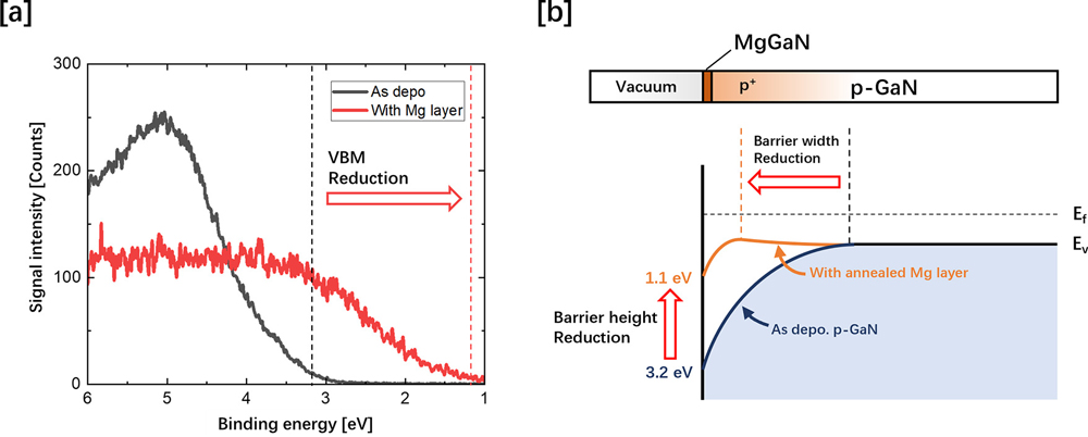
One factor reducing the barrier height and therefore improving Ohmic behavior was a reduced valence band maximum (VBM), as revealed by x-ray photoelectron spectroscopy (XPS, Figure 2). The p-GaN layer without Mg contact layer had a VBM of 3.2eV, which was reduced to 1.1eV with the annealed Mg/p-GaN process.

Figure 2: (a) VBM reduction determined by XPS measurement. (b) Surface band structure of as-deposited p-GaN (dark blue line) and p-GaN with annealed Mg layer (brown line).
Hall measurements gave a sheet resistance of 1.55x10⁵Ω/square, compared with 1.73x10⁵Ω/square without Mg contact. The Mg layer increased the sheet hole concentration (1.79x10¹²/cm2 versus 1.56x10¹²/cm2 ), while slightly depressing the mobility (22.5 and 23.2cm2/V-s, respectively).
Ohmic p-GaN Magnesium layer HBTs MOSFETs
https://doi.org/10.1063/5.0076764
The author Mike Cooke is a freelance technology journalist who has worked in the semiconductor and advanced technology sectors since 1997.


