News: Optoelectronics
4 April 2022
EU-funded project INSPIRE combining SiN and InP PICs with wafer-scale micro-transfer printing
After receiving nearly €5m in funding from the European°Union’s Horizon°2020 research and innovation program (under grant agreement n°101017088), the project INSPIRE was officially launched on 1 January.
Coordinated by Technical University of Eindhoven (TU/e) in the Netherlands and including imec, Thales, University of Cambridge, X-Celeprint, SMART Photonics, and Amires, the INSPIRE project consortium aims to change how photonic integrated°circuit (PIC) devices are fabricated in order to make them suitable for applications beyond communications (such as healthcare or sensing) and to speed up their large-scale production (overcoming existing limitations on scalability and high-throughput manufacturing).
In recent years there has been an upsurge in the use of photonic devices, based on materials including silicon, silicon°nitride (SiN) and indium°phosphide (InP), particularly for data°transfer applications, notes TU/e. While these devices have the potential for wider impact in other fields like sensors used in aircraft or communication devices, their uptake is limited since different materials need to be effectively combined to meet performance requirements.
For example, high-performance fiber°sensors used in infrastructure monitoring and microwave signal processing in radar systems require both low-noise operation and ultra-low degradation of signals. This can only be achieved through a combination of materials in the manufacturing process. If this manufacturing process can be properly scaled to allow large-scale production, it is expected that these photonic devices can have a major impact on sensing applications.
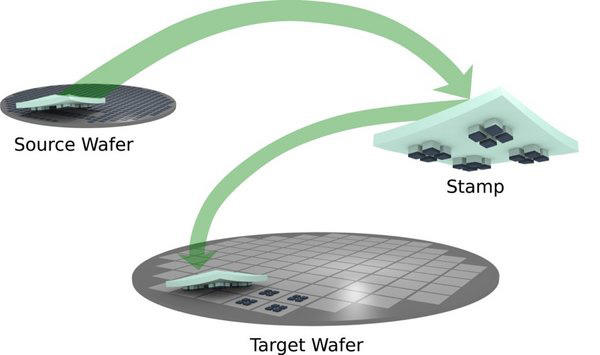
To facilitate the combination of these high-performance III-V optoelectronic materials in photonic devices, INSPIRE is developing wafer-scale micro-transfer printing technologies.
In micro-transfer printing, devices are first made on a source wafer, then transferred to a target wafer (see image). This printing concept has been established and widely applied by project partner X-Celeprint to different wafers and materials. The INSPIRE project is focusing on the next step: parallel device printing with accurate placement where many integrated devices can be printed at the same time.

The INSPIRE micro-transfer printing technology will be validated for three specific cases: fiber°sensors to measure stress, strain and temperature for use in airplane safety measures; a microwave photonic radio°frequency (RF) pulse generator with application in radar and wireless communication; and optical switches for energy-efficient data°centers. Compact versions of the III-V optoelectronic components will be developed, enabling designers to use this platform for a wide range of applications.
Combining established fabrication technologies
INSPIRE aims to consolidate established fabrication approaches, such as those from pure-play foundry and TU/e spinoff SMART Photonics and the silicon photonics pioneer imec, with the micro-transfer printing technology of X-Celeprint. This should result in a world-first fabrication platform that combines the strengths of two of the most well-known PIC manufacturing platforms. Methods will chiefly be developed for the coupling of SiN and InP processes, but could also be used for silicon-based photonics.
“By combining SMART and imec technologies, with only minor changes to the fabrication processes, we can leverage the major investments in the development of these platforms from the last decade,” says INSPIRE coordinator professor Martijn Heck of Eindhoven University of Technology. “We can thus significantly reduce the time needed to transfer our technology out of the lab, and make a faster and telling impact in new application areas,” he reckons.
Applications
The potential of the INSPIRE approach is demonstrated by the participation of industrial partners such as Dr°Jerome Bourderionnet of THALES: “The INSPIRE platform enables high-performance building°blocks, such as low-linewidth lasers, which are at the heart of THALES’ applications for optical signal processing at large, or sensing integrated systems,” he says.
INSPIRE aims to create a full-function PIC platform, compatible with open-access pilot manufacturing, and with an order-of-magnitude lower cost for volume production.
The INSPIRE consortium says that its generic approach makes the technology widely applicable and ensures that European innovators can focus their R&D directly on manufacturing platforms. As a result, it should take a shorter time to bring these PIC technologies to market.


