News: Optoelectronics
20 July 2021
PhotonicLEAP awarded over €5m in EU funding
The European collaborative project PhotonicLEAP has been awarded over €5m through the European Union’s Horizon 2020 program to develop photonics packaging and test technologies that should drive down the cost of photonics manufacturing.
Coordinated by Ireland’s Tyndall National Institute, the PhotonicLEAP consortium also consists of the research organizations and companies Fraunhofer (IZM & HHI), LPKF Laser & Electronic, ficonTEC Ireland, SUSS MicroOptics, BOSCH, Eindhoven University of Technology – TU/e and Interuniversitair Micro-Electronica Centrum – imec.
With demand for photonics being driven by mass-market technology requirements, the global photonics market is expected to exceed €850bn by 2026. In particular, photonic integrated circuit (PIC) technology is becoming increasingly important for existing markets in communications (high-speed fiber-optics), medical devices (e.g. cardiac diagnostics), sensors (e.g. in self-driving cars), a myriad of Internet of Things (IoT) technologies, and for emerging markets such as quantum computing and security.
However, existing PIC manufacturing processes, in particular packaging and test processes, are difficult to automate, with limited manufacturing capacity, and are costly, with packaging and testing typically accounting for over 75% of the total manufacturing cost. As a result, existing PIC manufacturing processes greatly impede the uptake of PIC technologies across many mass markets.
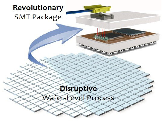
To address this challenge, the EU, through the PhotonicLEAP program, aims to develop wafer-level PIC module integration, packaging and test technologies that will reduce PIC production costs by over 10 times, revolutionizing existing applications and creating completely new markets.
Specifically, PhotonicLEAP will develop new technologies to produce a surface-mount technology (SMT) PIC package which, for the first time, incorporates multiple optical and electrical connections and can be scaled from low to very large volumes. The project will validate these technologies through two demonstrators, including a high-speed optical communication module and a portable medical device for cardio-vascular diagnostics. Furthermore, the technologies will be implemented by Europe’s flagship Photonic Integrated Circuits Assembly and Packaging Pilot Line (PIXAPP, which has an extensive and growing user-base across multiple markets), for future commercialization.

“Photonics is the key to unlocking the potential of technologies we need for today's interconnected world,” says Tyndall’s head of Photonics Packaging and Systems Integration professor Peter O’Brien, who will lead PhotonicsLEAP. “We need faster, more efficient, greener and cheaper solutions to our increasing usage of technology, which photonics manufacturing addresses. Therefore, we are delighted to receive this significant and vital funding from the European Commission to enable us to develop truly disruptive photonic packaging and test technologies,” he adds. The transnational consortium brings together “a wealth of photonics expertise, interdisciplinary skills and impressive infrastructure to deliver on our ambitious objectives,” O’Brien continues. “Packaging and test technologies developed in PhotonicLEAP can make a real impact to increase the uptake of integrated photonics across Europe.”


