News: Markets
4 August 2021
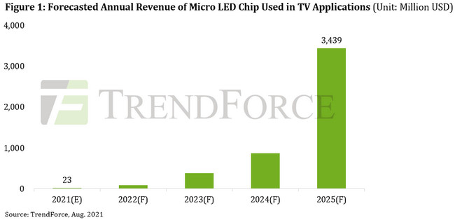
Micro-LED chip revenue for TVs to grow at 250% CAGR to $3.4bn in 2025
According to TrendForce’s report ‘2021 Mini/Micro LED Self-Emissive Display Trends and Analysis on Suppliers’ Strategies’, annual revenue of micro-LED chips for TV will rise at a compound annual growth rate (CAGR) of 250% to $3.4bn in 2025, due mostly to the early planning by display manufacturers to adopt micro-LED technology for large-sized displays.

Although the prohibitive cost of this technology is unlikely to be overcome in the short run, TrendForce still forecasts this revenue growth in light of several factors: first, micro-LED technology enables the production of gapless, large-sized modular displays; second, displays featuring micro-LED technology are able to meet the standards of cinema-grade displays or high-end TVs; finally, Korean TV brands have been aggressively investing in micro-LED TV development.
After TV market leader Samsung released its 146-inch TV wall (aptly named ‘The Wall’) in 2018, the company has continued to announce large-sized modular video walls and micro-LED TVs (which come in sizes such as 75-inch, 110-inch, 219-inch and 292-inch) at each subsequent Consumer Electronics Show (CES). TrendForce indicates that, prior to the widespread commercialization of micro-LED TVs, TV makers will continue to face challenges in terms of both technological barriers and costs. In particular, breakthroughs in three areas remain the most noteworthy: micro-LED chips, backplanes/drivers, and mass transfer.
With regards to cost, micro-LED chips comprise the highest share of micro-LED TV manufacturing costs, and their persistently high prices can be attributed to three factors. The first is the enormous number of chips used in TV manufacturing. For example, a 4K resolution TV requires 24.88 million micro-LED chips. Second, due to the diminutive size of micro-LED chips, their manufacturing process involves extremely stringent requirements regarding wavelength uniformity and cleanroom particle count. Finally, as micro-LED chips are smaller than 75μm, existing photoluminescence (PL) technologies are unable to fully detect defects in micro-LED chips, in turn increasing the difficulties in the mass transfer process of chips to backplanes.
With regards to backplane and driver technology, PCB backplanes paired with passive matrix (PM) are a relatively mature solution that has become the predominant choice for P>0.625mm pixel-pitch displays. However, for micro-LED TVs, which are smaller in size but maintain the same resolution, once their pixel pitch shrinks below 0.625mm challenges begin to arise with PCB backplane development, such as line width and line space, both of which can pose limits on mass production and increase manufacturing costs. Conversely, TFT glass backplanes paired with LTPS arrays are able to accurately control and drive the electrical circuits in micro-LED displays. This type of active matrix (AM)-equipped backplane is therefore expected to become the mainstream technology of micro-LED TVs going forward.
Another technological challenge in backplane development is glass metallization. As displays approach increasingly high resolutions, they require correspondingly smaller gaps between modules. Now that traditional COF (chip on film) designs are no longer viable, manufacturers are instead routing the wirings on the surface of the TFT glass either from the side or through TGV (through glass via) processes. In order to achieve this routing, manufacturers need to make use of glass metallization technology. However, as many technological bottlenecks still remain with regards to glass metallization (such as low yield rate and high cost), manufacturers must work to overcome these barriers as the industry moves forward.
In terms of manufacturing process, the main hurdles in micro-LED development are twofold: mass transfer and testing/repairing. The 24.88 million micro-LED chips used in each micro-LED TV pose an enormous demand in terms of mass transfer yield rate, manufacturing time, and testing/repairing processes. At the moment, the industry’s predominant mass transfer technologies consist of pick and place, laser transfer, fluidic assembly, magnetic mass transfer, roll-based transfer, and wafer bonding. The adoption of each respective mass transfer technology depends on the resolution of the display products as well as the size of micro-LED chips to be transferred, and each of these technologies comes with its own impact on production capacity, yield rate, and manufacturing equipment costs. That is why micro-LED production lines involve such a high degree of complexity. TrendForce believes that the mass transfer process in micro-LED TV manufacturing needs to reach a rate of at least 20 million UPH (units per hour) and a 99.999% yield for micro-LED TVs to be viable for wide commercial release.


