| Home | About Us | Contribute | Bookstore | Advertising | Subscribe for Free NOW! |
| News Archive | Features | Events | Recruitment | Directory |
| FREE subscription |
| Subscribe for free to receive each issue of Semiconductor Today magazine and weekly news brief. |
News
14 November 2006
Toshiba announces record-breaking GaN power FET
Toshiba Corporation claim to have developed GaN power field effect transistors (FETs) that exceed the operating performance of GaAs FETs used in microwave solid-state amplifiers for radar and satellite microwave communications in the 8GHz to 12GHz X-band frequency range. According to Toshiba, its new transistor achieves an output power of 81.3W at 9.5GHz, a record at this frequency, and six times the power density of a GaAs FET.
Toshiba says the breakthrough was achieved by optimizing the epitaxial layer and chip structures for X-band operation. The company began by optimizing the composition and the thickness of the AlGaN and GaN layers. Then, working with the epitaxial layer structure, the FET unit structure (including gate length and the distance between the source and drain electrodes) was optimized. In order to produce a high-level of performance at X-band, Toshiba says that the FET requires a gate electrode under 0.5 micron meter, and that the suppression of current leakage at the gate electrode is essential. The company adds that its “unique” gate electrode structure and overcoat process helps suppress gate leakage to 1/30th of conventional technology.
 Section of GaN power FET chip.
Chip size: 3.4 mm x 0.53 mm
Instead of the electron beam exposure technology often used in lithography processes for GaN power FETs at the C-band and higher frequencies, Toshiba has adopted stepper exposure that it claims is better suited to the mass production of X-band FETs that require a gate length of less than 0.5 microns.
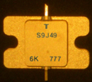
 Power GaN FET
external dimensions: 21.5mm x 12.9mm
The company says that this breakthrough opens the way to even higher frequency levels in the 12GHz to 18GHz (Ku-band).
Visit: http://www.toshiba.co.jp