| Home | About Us | Contribute | Bookstore | Advertising | Subscribe for Free NOW! |
| News Archive | Features | Events | Recruitment | Directory |
New MEMS White Paper
Download the latest Logitech white paper and learn more about MEMS processing technology and techniques
| FREE subscription |
| Subscribe for free to receive each issue of Semiconductor Today magazine and weekly news brief. |
News
27 March 2007
IBM demonstrates record-speed 160Gb/s optical chipset
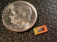
At this week’s 2007 Optical Fiber Conference in Anaheim, CA, USA, IBM's T. J. Watson Research Center of Yorktown Heights, NY, USA is presenting a prototype optical transceiver chipset capable of transmitting data at a record speeds (for a single, integrated transceiver chip) of 160Gbit/s. This is at least eight times faster than optical components currently available, claims the firm (‘160-Gb/s, 16-Channel Full-Duplex, Single-Chip CMOS Optical Transceiver’ by C.L. Schow et al).
“The explosion in the amount of data being transferred, when downloading movies, TV shows, music or photos, is creating demand for greater bandwidth and higher speeds in connectivity,” says Dr T.C. Chen, VP, Science & Technology, IBM Research. “Greater use of optical communications is needed to address this issue.” The transceiver is fast enough to reduce the download time for a typical high-definition feature-length film to a single second compared to 30 minutes or more over the best available connectivity today, IBM says.
By shrinking and integrating the components into one package, and building them with standard low-cost, high-volume chip manufacturing techniques, optical connectivity viable for widespread use, reckons IBM. The technology could be integrated onto printed circuit boards to allow the components within an electronic system - such as a PC or set top box - to communicate much faster, dramatically enhancing the performance of the system itself.
 To achieve this level of integration in the chipset, IBM researchers built an optical transceiver with driver and receiver ICs in current CMOS technology, coupled with InP- and GaAs-based optical components (including a 4x4 VCSEL array) in a single, integrated package just 3.25mm by 5.25mm in size.
The compact design provides both a high number of communications channels as well as very high speeds per channel, resulting in a record amount of information transmitted per unit area of card space taken up by the chipset. The transceiver chipset is designed to enable low-cost optics for computing-intensive applications by attaching it to an optical PCB employing densely spaced polymer waveguide channels using mass assembly processes.
* The work was partially funded by the US Defense Advanced Research Project Agency through the Chip to Chip Optical Interconnect (C2OI) program.
Visit: http://www.research.ibm.com