- News
26 September 2019
Indium gallium arsenide one-transistor dynamic random access memory
Spain’s University of Granada and IBM Research Zürich in Switzerland have been developing III–V on silicon technology for dynamic random access memory (DRAM) based on one transistor (1T) and without a capacitor structure [Carlos Navarro et al, Nature Electronics, published online 19 August 2019]. The team comments: “Such capacitor-less DRAM has been demonstrated in silicon, but the use of other materials, including III–V compound semiconductors, remains relatively unexplored, despite the fact that they could lead to enhanced performance.”
Removing the capacitor used in traditional ‘1T1C’ DRAM allows simpler processing and should enable smaller cell sizes. The increased carrier mobility in III–V compound semiconductors such as indium gallium arsenide (InGaAs) offers the prospect of lower operating voltages and lower energy consumption.
The researchers describe their structure as being related to the meta-stable dip RAM (MSDRAM) concept that uses parasitic floating-body effects (FBEs) to store information. FBEs arise in semiconductor-on-insulator (-OI) structures where the potential in the semiconductor depends on biasing history and carrier recombination processes. The charge in the body of the device modulates current flow in the reading operation.
The team sees potential uses of the device coming from demands for higher performance and scalability, along with III–V optoelectronics and high-power circuitry.

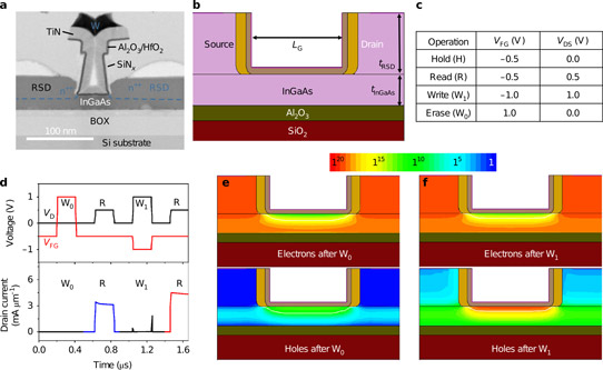
Figure 1: a, Transmission electron microscope image of III–V cell. b, Corresponding 2-dimensional structure used in simulations. c, Default front-gate (VFG) and drain (VD) voltages for memory operation. d, Readout drain current, demonstrating memory operation. Inset: drain and front-gate bias pattern. e,f, Electron and hole densities, after W0 (e) and W1 (f), respectively, demonstrating MSDRAM memory operation in structures similar to experimental devices with 5V on back gate. Simulated device dimensions: 90nm LG, 1μm width.
The devices were based on InGaAs-OI transistors fabricated on silicon at IBM’s Zurich facility (Figure 1). The InGaAs channel layer was 20nm thick. The indium mole fraction was 53%, which provides a good trade-off between the on- and off-current performance through a high electron mobility and a relatively wide bandgap.
InGaAs-OI on silicon wafers were direct bonded structures using metal-organic chemical vapor deposition (MOCVD) heterostructures grown on indium phosphide (InP) transferred to (001) silicon. The buried oxide layers (BOX) were added by atomic layer deposition (ALD) onto the InP growth wafer, which was then flipped onto the silicon for initial bonding, followed by annealing. The InP growth substrate, and etch stop layers, were then removed.
The aluminium/silicon BOX layers (10nm/25nm Al2O3/SiO2) prevents charge leaked into the p-Si substrate. The back-side of the wafer served as a back gate electrode. A front gate was implemented with 4nm-total high-k aluminium/hafnium oxide (Al2O3/HfO2) bilayer, giving a 1nm equivalent oxide thickness (relative to the traditional SiO2).
The MSDRAM principle uses coupling between the front- and back-gates, along with floating-body and non-equilibrium effects. The gates create front- and back-channels. Holes accumulate in the front-channel, while the back-channel is driven into inversion by the back-gate. The accumulated holes modulate the electron density in the inverted back-channel. Larger hole density in the front-channel enables increased current flow in the inversion layer.
The ‘0’ state is written (W0 or ‘erase’) by applying a positive potential to the front-gate, expelling holes from the front-channel through capacitive coupling. The ‘1’ state (W1 or ‘write’) is created through band-to-band tunneling to inject holes from the drain edge with a negative front-gate potential and positive drain bias.
The MOCVD regrown n-type source/drain regions were raised 25nm and isolated from the gate stack with 9nm plasma-enhanced ALD silicon nitride spacers. The doping of the source/drain with tin was 2x10¹⁹/cm3. The channel body suffered in performance due to some residual n-type doping of the order 2x10¹⁶/cm3. This factor modified the desired MSDRAM behavior, to give something more approaching what is described as an ‘A2RAM’.
Final devices with various gate lengths (LG) were fabricated with a 0.5μm width. The subthreshold swings with the back-gate at 0V were ~150mV/decade and ~200mV/decade for 90nm and 14nm gate length, respectively. The relatively high swings were attributed to “interface defects at the gate/channel interface”. The higher value for the 14nm device also indicated the presence of short-channel effects in the highly scaled device.
Putting a positive voltage on the back-gate switches the channel for current flow from the top to the back interface. This flattens the control of current flow by the top-gate. Due to the thick BOX layer, the current control by the back-gate is limited. However, the current in the back channel is modulated by charge trapped in the front channel, creating the prospect of 1T-DRAM performance (Figure 2).

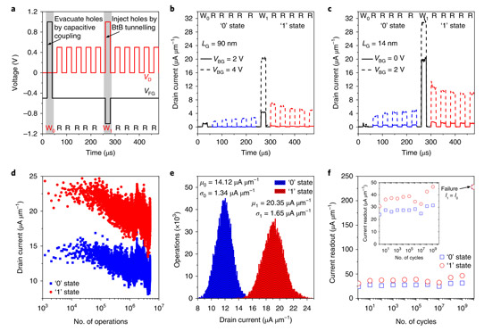
Figure 2: a, Default W0−5×R–W1−5×R sequence bias pattern to test memory operation. b,c, Readout drain current, successfully probing the memory behavior for 90nm (b) and 14nm LG (c) at room temperature (300K). d,e, Endurance test on 50nm LG device at high temperature (360K), showing continuous ‘0’- and ‘1’-state readout currents for the first 5x10⁶ cycles (one in every 100 points) (d), together with Gaussian-shaped histograms (e). f, Longer cycling test showing memory operation up to between 109 and 1010 cycles when successive ‘1’-state writing steps are carried out at 50MHz. State current readouts characterized every decade. Inset: magnified view of memory operation.
The reading of the memory state was through a drain bias. Due to the residual body n-type doping, there was still a significant current flow for the ‘0’ state, although the ‘1’ state did demonstrate a higher value. Write and erase processes involved specific front-gate voltage pulses.
To test the endurance of the cell, a 50nm-gate device was subjected to 5x10⁶ cycles of a sequence of W0-R-W1-R operations at 360K without bit failure. The back gate was set at 5V. The various front-gate potentials were −0.3 V (R), −0.8V (W1), and +0.8V (W0). The pulse widths were 20μs. The researchers comment that basic calculations suggest that endurance of 5x10⁹ operations could be envisaged with nanosecond-order operations. Another test at 360K with 50MHz W1 operations, considered the most damaging, only failed after 109-1010 cycles.
https://doi.org/10.1038/s41928-019-0282-6
The author Mike Cooke is a freelance technology journalist who has worked in the semiconductor and advanced technology sectors since 1997.


