- News
4 July 2019
Ultra-low-power light-emitting diodes for Internet of Things and smart dust
IBM T J Watson Research Center and University of California Berkeley in the USA report on extending high efficiency to lower-current light-emitting diode (LED) performance [Ning Li et al, Nature Photonics, published online 17 June 2019].
The researchers see opportunities for ultra-low-power (LP) performance leading to wireless communication in smart dust and sensor networks, low-cost block chain and authentication security, and medical applications. They further reference ‘Internet of Things’ (IoT) development of low-cost, self-powered dust-sized components with power requirements limited to the microwatt level due to energy supply considerations. Unfortunately, radio-frequency devices need milliwatt-level input power and suffer a size mismatch between antennas and wavelengths.
“Miniaturization to this dust-sized platform is possible because of the remarkable advancements in microelectronics technology and micro-packaging, which allow system-level integration of energy-harvesting devices, microprocessors and memories, and wireless communication devices, all within a small footprint,” the team comments.
Th epitaxial structures were grown by metal-organic chemical vapor deposition (MOCVD) on semi-insulating gallium arsenide. The emission layer consisted of a strained single indium gallium arsenide (In0.2Ga0.8As) quantum well in indium gallium phosphide (In0.49Ga0.51P) barriers. The barriers featured 50nm undoped confinement layers and 200nm lightly-doped materials next to the heavily doped contacts (1000nm n-GaAs buffer, 30nm p-GaAs).
The team designed the structure to reduce the interface recombination velocity and increase hole density in the well at low current injection (Figure 1). The high-quality interface reduced non-radiative recombination there. A large valence band offset with the barriers created a deep well for holes to gather in, exceeding the electron density. The high hole concentration favors radiative over non-radiative recombination.

Figure 1: Structure and design of the LP-LED: schematic representation of structure (a) and band diagram (b) with high valence-band offset; (c) cross-sectional transmission electron microscopy image of epitaxial layers.
Fabrication included wet etching of circular mesas. The mesa sidewalls were passivated with atomic layer deposition (ALD) aluminium oxide. The GaAs substrate was transparent to the emission from the well, enabling the use of flip-chip assembly onto silicon with light extraction through the back-side of the chips.
The devices were compared with LEDs fabricated from three other structures: Al0.2Ga0.8As/In0.2Ga0.8 As and Al0.3Ga0.7As/GaAs barrier/single quantum wells, and a commercial multiple quantum well product. The in-house comparison devices used the same barrier/well thicknesses as the LP-LED.
The InGaAs/InGaP LP-LED achieved 80% of the peak efficiency at 0.1μA injection (1mA/cm2) and 40% at 1nA (10μA/cm2). The comparison device efficiencies fell off rapidly in the range 0.1-1mA.
The LP performance was improved by increasing the device diameter from 120μm to 960μm. The larger-diameter LP-LED was able to maintain near peak efficiency below 0.1mA/cm2 injection density [my calculation: 0.64mA]. The improved performance was attributed to reduced non-radiative recombination at the mesa side walls.
The researchers commented: “Previously reported devices only reach high efficiency at currents on the scale of millliamps, while our device has near-unity efficiency at a low current of 1μA.” Although the device demonstrated a peak external quantum efficiency of only 7%, this was limited by light extraction out of the GaAs substrate. Optical simulations suggest that, even with perfect 100% internal quantum efficiency, only 8% of the light could be extracted.
The estimated internal quantum efficiency remained high – more than 90% at 1V forward bias – even well below the photon voltage of 1.3V (photon energy/electron charge), equivalent to a wavelength of 954nm in the near-infrared range (750nm-1400nm). The 1V level is easily achievable with mainstream silicon complementary metal-oxide-semiconductor (CMOS) circuitry, unlike the higher 1.3V level that needs special charge pumping and current drivers.
The researchers comment: “Although conventional LEDs commonly show some light emission when biased below the photon voltage, efficiency is very low because the non-radiative process dominates.”
The team also speculates that electroluminescent cooling could be achieved if the light extraction was better than 93%, which they say is achievable in some schemes aimed at avoiding light being trapped in the device.
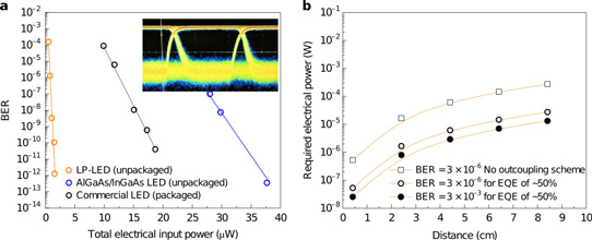
Free-space data transmission also showed much improved bit-error rates for given operating power (Figure 2). The team comments: “A detector noise analysis shows that the required optical power is quite low with proper optical filtering and the right photodetector. This yields significant transmitter power savings (>100×) compared to conventional LEDs at distances of 0–10cm, relevant for many low-power IoT and smart dust applications. Compared with the previously reported best RF transmitters with small footprint, the power consumption is orders of magnitude lower for the LP-LED.”

Figure 2: Data transmission performance at low current and voltage: (a) bit-error rate (BER) versus input power for unpackaged LP and AlGaAs/InGaAs LEDs, and commercial packaged device. Inset: eye diagram of LP-LED at 1μW input power and 1V bias. (b) Required electrical input power for the LP-LED versus distance to reach BERs of 3x10⁻⁶ and 3x10⁻³ without and with enhanced light outcoupling. Clock frequency 1MHz.
Asynchonous transmission of a text file from a computer to a smartphone was also demonstrated. The average current was 0.92μA and the voltage swing was 0-1.2V. The average power consumption was 1.1μW. The transmitted 1Mbyte text file was error-free, giving a bit-error rate of less than 10-6. The transmission rate of 100 kilobits per second was limited by the phone software.
The device was flip-chip bonded to solder bumps on silicon. Such a silicon carrier could also contain a microprocessor, memory, power, receiver, and other electronic systems. The present device fitted a 1mmx1mm format.
https://doi.org/10.1038/s41566-019-0463-x
The author Mike Cooke is a freelance technology journalist who has worked in the semiconductor and advanced technology sectors since 1997.


