- News
27 December 2019
Gallium arsenide photodetector on thin germanium-on-silicon virtual substrate
Researchers based in United Arab Emirates have used germanium-on-silicon templates to produce gallium arsenide (GaAs) metal-semiconductor-metal (MSM) photodetectors [Ghada Dushaq et al, J. Appl. Phys., vol126, p193106, 2019]. The team from New York University Abu Dhabi, and from Khalifa University, comments: “The extension of this method to other III–Vs and lattice-mismatched systems may enable high-performance optoelectronics in visible and near-infrared bands.”
Monolithic integration of III-V materials on silicon is also hoped to reduce costs with high yields and production volumes, and further allowing combination with mainstream complementary metal-oxide-semiconductor (CMOS) electronics and silicon photonics platforms.
III-V materials like GaAs are more optically active than indirect-bandgap silicon. GaAs and other materials thus have higher photodetection performance. In addition, the creation of efficient light sources – LEDs and lasers – overwhelmingly mandates the use of direct-bandgap materials, the most highly developed of which are the III-V class of compound semiconductors.
The deposition of III-V materials on silicon is hampered by mismatched lattice and thermal expansion parameters. In their work, the researchers used a germanium layer that was much thinner than the ~10μm graded silicon germanium layers often employed to bridge between silicon and III-V semiconductors.
The germanium-on-silicon template or ‘virtual substrate’ consisted of a 700nm radio-frequency plasma-enhanced chemical vapor deposition (PECVD) layer on (100) silicon. The GaAs came from a metal-organic chemical vapor deposition (MOCVD) process involving tertiarybutylarsine (TBA) and trimethylgallium (TMGa) precursors.
Before the GaAs deposition the Ge surface was baked at 400°C and 700°C for 5 min and 10 min, respectively. The aim of these thermal treatments was to enable the transition from non-polar Ge to polar GaAs without introducing antiphase boundaries (APBs), dislocations and stacking faults. The researchers describe the treatment as “an essential step toward increasing the density of double atomic steps, adsorbing the Ge native oxide, and enhancing surface quality before starting the GaAs deposition.”
The GaAs was deposited in two steps: at 500°C for 5 minutes, creating a seed layer, and then at 550°C for the remainder of the growth. The device layer was undoped, aiming at intrinsic conduction behavior with a view to low-voltage operation. In fact, interdiffusion of germanium into the GaAs layer introduced trapping states and extended defects that gave p-type conduction with 5x10¹⁷/cm2 hole concentration, resulting in a sheet resistance of ~200mΩ/square.
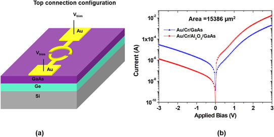
The GaAs surface was cleaned and subjected to oxygen plasma treatment before passivation with 1-2nm of sputtered aluminium oxide (Al2O3), which targeted a good-quality Schottky contact. Evaporated chromium (Cr) and gold (Au) were used as the metal contacts of the MSM photodetector. The 15nm chromium acted as an adhesion and seed layer for the gold contact.

Figure 1: (a) Top electrical connection of GaAs MSM detector and (b) current-voltage rectifying behavior at metal-semiconductor junction with/without Al2O3 interlayer.
The Al2O3 interlayer reduced leakage in the Schottky junction by a factor of ~20 at 1V reverse bias (Figure 1). The on/off current ratio with Al2O3 passivation was around 103 for ±1V bias. The interlayer also reduced the Schottky barrier height to 0.62eV, compared with 0.67eV without Al2O3 passivation.
The interlayer avoided the severe Fermi-level pinning resulting from bare-surface GaAs defect states. Further the aluminum oxide improved photon collection efficiency.
The dark current density in devices of 30-140μm diameter was ~6mA/cm2 .

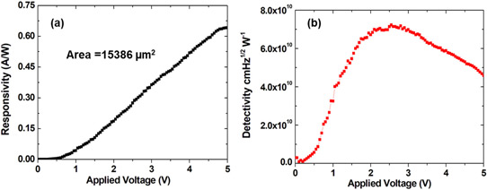
Figure 2: (a) Responsivity and (b) detectivity as function of reverse bias voltage.
The optical response was measured using 850nm monochromatic laser light (Figure 2). Passivated and unpassivated devices had similar response characteristics. The passivate device was superior in terms of reduced dark current. The responsivity at 5V reverse bias was as high as ~0.54A/W. The researchers estimate an 85% quantum efficiency. Variation in response of different devices ranged between 0.4 and 0.64A/W.
The researchers compared their response with theoretical expectations of 0.41A/W, based on the bulk GaAs absorption coefficient. The ~1.55x enhancement measured in the experiments on the 0.64A/W device is attributed to an increased absorption in the non-bulk GaAs body of the device.
The researchers comment: “In the theoretical calculation, we considered the absorption coefficient of bulk GaAs. However, in the heteroepitaxy thin-film GaAs structure, the optical parameters are significantly affected by growth condition, layer thickness, and the material beneath it. Additionally, Ge is a highly absorbent material at 850nm.”
In particular, the team points to x-ray analysis showing that the Ge and GaAs layers are tensile strained. The researchers believe the strain leads to increased absorption of light from a reduced energy bandgaps. A further 1.5% boost is attributed to light reflected at the GaAs/Ge interface.
The detectivity, extracted from photo-current and dark-current responses, was ~4.6x1010cm-Hz1/2/W.
The junction capacitance was ~500fF at 1V reverse bias. The researchers say that the small capacitance means that the bandwidth of the device is limited instead by the carrier transit time across the device. The team estimates the 3dB bandwidth at up to 9GHz, and around 4GHz with 1V bias.
Reduced response time could result from scaling down the device, but there is a trade-off from reduced photoresponse with decreased active area. The trade-off could be improved with transparent electrodes.
Germanium-on-silicon templates GaAs metal-semiconductor-metal photodetectors GaAs CMOS MOCVD PECVD
https://doi.org/10.1063/1.5120705
The author Mike Cooke is a freelance technology journalist who has worked in the semiconductor and advanced technology sectors since 1997.


