- News
3 April 2019
Tailoring defects in bismuth sulfide yields highly sensitive CMOS-compatible broadband IR photodetector
There is keen demand in the consumer electronics sector for infrared optoelectronics including light-emitting diodes and photodetectors. But, to date, infrared optoelectronics have been served by costly CMOS-incompatible III-V semiconductors. Recently, a new class of semiconductors that address the CMOS compatibility issue has emerged based on colloidal quantum dots. For consumer electronics the use of RoHS-compliant materials is a prerequisite and there is hence a strong need for the development of high-performance devices based on environmentally friendly elements (which had remained elusive in the infrared).
To address this challenge, Institut de Ciències Fotòniques (ICFO – the Institute of Photonic Sciences) in Barcelona, Spain has discovered that, by controlling defects in materials, one can extend the semiconductor’s spectral reach beyond its bandgap, expanding the material availability for the infrared part of spectrum (‘Engineering Vacancies in Bi2S3 yielding Sub‐Bandgap Photoresponse and Highly Sensitive Short‐Wave Infrared Photodetectors’, Advanced Optical Materials; DOI: 10.1002/adom.201900258). In work supported partially by the European Commission’s Graphene Flagship initiative, ICFO researchers Dr Nengjie Huo, Dr Alberto Figueroba, Dr Y. Yang, Dr Sotirios Christodoulou, Dr Alexandros Stavrinadis, led by ICFO’s ICREA (Catalan Institution for Research and Advanced Studies) Research Professor/group leader Gerasimos Konstantatos, in collaboration with professor C. Magén of University of Zaragoza, have reported the development of an infrared detector using bismuth sulfide. This has proven to have fast and high photo-response levels in the short-wave infrared range due to the formation of defects in the material.
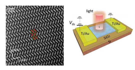
In the experiment, the team fabricated a photoconductive detector, depositing a very thin layer of Bi2S3 flakes onto a Si/SiO2 substrate. It was then observed that the Bi2S3 flakes were sulfur-deficient (with sulfur vacancies or defects in the material), creating extended in-gap states, which allowed increased absorption of light below the bandgap value of Bi2S3 (i.e. sub-bandgap). Such features led to a high-gain, low-noise and, consequently, a high-sensitivity photodetector.

Picture: Left: STEM image of crystal: red and green balls represent bismuth and sulfur atoms. Right: schematic illustration of Bi2S3 detector on Si/SiO2 substrate.
To give insight into the sulfur deficiency mechanism, the team fabricated a second photodetector and synthesized the Bi2S3 crystal by performing a sulfurization process (changing the proportions of Bi and S in the crystal) and subsequently refilling the sulfur vacancies. The photodetector was seen to have a much faster response time but was limited to the near-infrared spectral range. Thus, to improve the response time without sacrificing its spectral coverage into the infrared, the team carried out a mild chemical treatment on the sulfur-deficient-based detector, through a process of surface passivation of the crystal. It was subsequently seen that the time response had reached about 10ms for the infrared and visible light range, 50 times faster than the original sulfur-deficient-based detector.
It is reckoned that the results of the study provide new insight into the role that atomic vacancies play in electronic structure and how sub-bandgap photoresponse effects can enable ultra-sensitive, fast and broadband photodetectors.
https://onlinelibrary.wiley.com/doi/abs/10.1002/adom.201900258
www.icfo.es/lang/research/groups/groups-details?group_id=30


