- News
17 October 2018
Orienting quantum cascade lasers to higher efficiency and lower threshold
Humboldt University Berlin and Paul-Drude-Institut für Festkörperelektronik in Germany have used (411)A oriented indium phosphide (InP) to improve the power efficiency, threshold current and slope efficiency of quantum cascade lasers (QCLs) [M. P. Semtsiv et al, Appl. Phys. Lett., vol113, p121110, 2018]. The material aimed at 9μm wavelength emission used combinations of indium gallium arsenide (InGaAs) and indium aluminium arsenide (InAlAs) layers.
The researchers attribute the improvements to reduced interface roughness (IFR) scattering enabled by growth on (411)A material, compared with conventional on-axis (100) substrates. “A reduced IFR scattering results in better inversion, longer upper laser state lifetime, smaller non-radiative recombination, and less leakage current during injection,” the team reports.
The improvements are thought to result from the change in average lateral extent of the roughness, rather than the height/amplitude. The lateral extent for the conventional (100) orientation is around 6nm, which gives expect peak expected IFR scattering in devices aimed at 9-20μm wavelength emission.
The researchers report that, although off-cut substrates like (411)A InP are commonly used to achieve almost atomically flat epitaxial growth fronts, they had not been previously applied in QCL work. The team explains: “The off-cut substrates introduce monolayer-high steps into the growth front, but these steps are more regular than the random monolayer-high islands on the exact (100) surface, and are characterized by a different lateral size Λ. Growth proceeds in the step-flow mode, reducing fluctuations with random lateral extent.”
The (411)A orientation is tilted 19.5° relative to the convention (100) surface plane in the [011] direction. The flat surface morphology during epitaxy has typically 1.8nm long terraces in the [-122] direction, much shorter than the 6nm ‘lateral extent’ seen for the (100) orientation. Previous work characterizing such material confirmed improved qualities such as higher electron mobility and a narrower photoluminescence peak.
The epitaxial wafers were produced on InP substrates with conventional (100) and with (411)A surface orientations. The QCL epitaxial structure, based on a design by Hamamatsu Photonics K.K. researchers, was an InGaAs/InAlAs heterosystem lattice-matched to InP, giving a dual-upper-state to multiple-lower-state active regions. The growth temperature was 500°C.
The material was fabricated into lasers with ~30μm-wide ridges. For the (411)A the ridge was oriented along the [1-10] crystal direction, allowing cleavage along the perpendicular direction to give mirror facets. The ridge sidewalls were insulated with silicon dioxide. The top and bottom electrodes were annealed chromium/gold and gold-germanium/chromium/gold, respectively. The devices were soldered onto copper-tungsten submounts.
Although the devices operated at room temperature and above, the reported measurements were restricted to the stable 60-280K range of the team’s cryostat equipment. The team believes, however, that the efficiency improvements enabled by growth on (411)A InP could result in higher maximum operation temperatures.

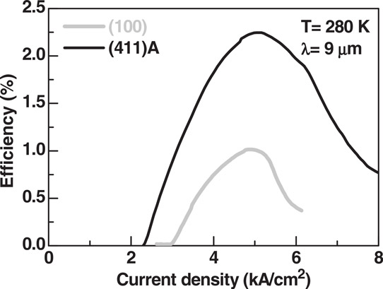
Figure 1: Power (wall plug) efficiency as function of current density with same QCL structures grown on (411)A and (100) oriented InP. Both lasers were 4mm long. Lasers grown on (411)A and (100) substrates had 24.4μm- and 32.7μm-wide ridges, respectively.
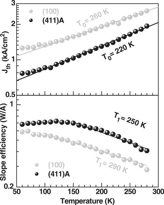
The (411)A device demonstrated more than twice the maximum ‘wall-plug’ power efficiency at 280K under 150ns pulsed operation with 10kHz repetition, compared with the reference (100) QCL (Figure 1). The improvement is credited to reduced interface roughness scattering. The threshold currents of the (411)A devices were also lower (Figure 2). However, the lower characteristic temperature for the threshold (T0) for the (411)A QCL does mean that the threshold does approach that of the conventional (100) laser at higher temperatures. The researchers attribute this to “an increasing influence of phonon scattering”.

Figure 2: Top: Threshold current densities as functions of temperature for QCLs on (411)A and (100) InP. Bottom: slope efficiency functions of temperature. In both panels, bullets are experimental data and lines are simple exponential fits.
Above 150K the slope efficiency of the (411)A device was about 50% higher than that of the (100) structure. The saturation of the (411)A QCL’s slope efficiency below 150K was probably due to freeze-out of carriers as a result of the low doping used in the design, the researchers suggest. A (411)A QCL with wider 33.2μm ridge had similar temperature characteristics: 217K for T0, and 234K for the slope efficiency (T1).
https://doi.org/10.1063/1.5049090
The author Mike Cooke is a freelance technology journalist who has worked in the semiconductor and advanced technology sectors since 1997.


