- News
24 July 2018
GaAs wafer market growing at 15% CAGR to 2023, driven by photonics applications growing at 37%
© Semiconductor Today Magazine / Juno PublishiPicture: Disco’s DAL7440 KABRA laser saw.
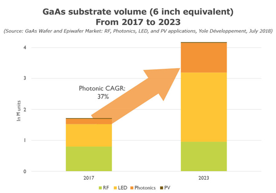
After a quiet period due to the saturation of the mobile handset industry, the gallium arsenide (GaAs) wafer market is rising at a compound annual growth rate (CAGR) of 15% (by volume) between 2017 and 2023, including 37% for photonics applications in particular, according to the report ‘GaAs Wafer & Epiwafer Market: RF, Photonics, LED and PV applications’ from Yole Développement.
As one of the most mature compound semiconductors, GaAs has been ubiquitous as the building block of power amplifiers in every mobile handset. In 2018, GaAs radio frequency (RF) business represents more than 50% of the GaAs wafer market. However, in the past couple of years growth has slowed due to the handset market’s gradual saturation and shrinking die size. “With the transition from 4G to 5G, we expect GaAs to remain the mainstream technology for sub-6GHz instead of CMOS, owing to GaAs’ high-power and linearity performance as required by carrier aggregation and MIMO technology,” says technology and market analyst Dr Hong Ling.
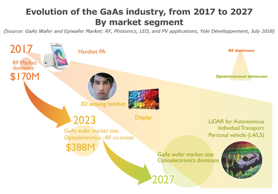
Since 2017, GaAs wafers have been particularly notable in photonics applications. When Apple introduced its new iPhoneX with a 3D sensing function using GaAs-based vertical-cavity surface-emitting lasers (VCSELs), it paved the way for a significant boost in the GaAs wafer market segment for photonics applications, which should grow at a CAGR of 37% to about $150m by 2023.

“GaAs-based ROY [red-orange-yellow] and infrared light-emitting diode applications have also caught our attention,” says technology and market analyst Dr Ezgi Dogmus. For the total GaAs LED market, Yole forecasts a 21% CAGR, surpassing more than half of GaAs wafer volume by 2023.
In terms of wafer and epiwafer business, each application requires a different size and quality when determining prices. As a new entrant, photonics applications will impose new specification requirements compared with the well-established RF and LED wafers and epiwafers, creating significant diversity in average selling price (ASP).
GaAs photonics: smartphones today, automotive tomorrow?
The GaAs wafer and epiwafer markets are now entering a new era, with optoelectronics taking the limelight from RF applications. Not too long ago, GaAs photonics was a relatively tiny market whose principal application was data centers. But ever since the introduction of a 3D sensing function using GaAs-based VCSELs in Apple’s iPhone X, GaAs VCSELs have attracted huge attention. Indeed, three sensor modules based on GaAs VCSELs are used in the iPhone X for facial recognition: (1) a proximity sensor for activity/human detection; (2) a flood illuminator for face and eye detection in daytime or night; and (3) a dot projector for facial recognition. With potential adoption of this technology by Android platforms, Yole expects this GaAs wafer market segment for VCSELs to grow at a remarkable 58% CAGR over 2017-2023.
Moreover, the GaAs photonics market is not limited to VCSEL applications. Light detection and ranging (LiDAR) is a key technology allowing the creation of a 3D map of surroundings for autonomous vehicles and robotics. This emerging application uses high-power and large-size GaAs-based edge-emitting laser (EEL) devices, which will represent an incredible boost for the GaAs photonics wafer market, says Yole.

Along with the GaAs photonics wafer market’s remarkable growth, ROY and infrared LEDs on GaAs substrates are expected to show strong growth potential. Large-display, automotive and horticultural lighting applications are the main drivers for red LEDs, posting a CAGR of 21% over 2017-2023 for the ROY GaAs wafer market. Similarly, GaAs-based IR-LEDs used in medical sensors for blood pressure and blood sugar, as well as proximity sensors for gesture recognition in smartphones and automotive, are also growth segments of the market.
Industrial players embracing the new era
From the point of view of the value chain, the GaAs photonics market’s remarkable growth potential will offer plenty of opportunities for wafer and epiwafer suppliers as well as metal-organic chemical vapor deposition (MOCVD) equipment suppliers, and investors.
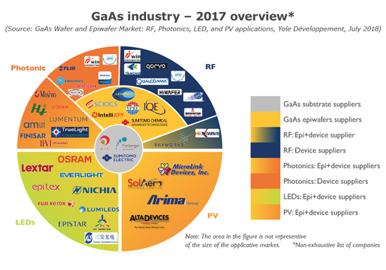
In terms of GaAs wafer supply, Sumitomo Electric, Freiberger Compound Materials and AXT lead the market, with a collective market share of about 95%. Also, since new laser applications have very high-specification requirements for GaAs wafers that are constantly evolving, Yole expects the top players to maintain their technical advantage for at least another 3-5 years.
Meanwhile, Chinese GaAs wafer suppliers like Vital Materials, which have captured part of the LED market from the leading suppliers, are expected to increase their share thanks to LED markets.

Regarding GaAs epiwafer production, Yole identifies different business models. The GaAs LED market is principally vertically integrated, with very well-established integrated device manufacturers (IDMs) like Osram, San’an, Epistar and Changelight. In parallel, GaAs RF businesses outsource significantly from well-established epi houses.
Over the last few years, the GaAs RF epi sector has gone through much consolidation, resulting in four main players: IQE, VPEC, Sumitomo Chemicals (including Sumitomo Chemical Advanced Technologies and SCIOCS), and IntelliEPI.
Regarding the GaAs photonics sector, the epi business is still application-dependent. The GaAs datacom segment is mostly epi-integrated, with dominant IDMs like Finisar, Avago and II-VI. For 3D sensing in smartphones, epi outsourcing is significant.
In 2017, Apple’s supplier Lumentum used IQE as its VCSEL epi supplier. This resulted in an almost 10x increase in IQE’s stock price. Other leading GaAs epi houses are in qualification or ramping up. Yole concludes that it expects the photonic epiwafer market to behave similarly to the GaAs RF epiwafer market.
GaAs substrates GaAs epitaxial wafers
www.i-micronews.com/compound-semi-report/


