- News
5 July 2018
Undoped gallium nitride upper waveguide for reduced laser threshold
Researchers in China have used an undoped gallium nitride (u-GaN) upper waveguide (WG) to reduce the threshold current density for an indium gallium nitride (InGaN) laser diode (LD) [Feng Liang et al, Jpn. J. Appl. Phys., vol57, p070307, 2018].
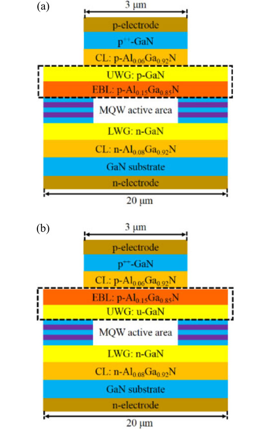
The u-GaN waveguide was positioned between the last quantum barrier of the multiple quantum well active region of the device and the p-type aluminium gallium nitride (p-AlGaN) electron-blocking layer (EBL). This reverses the conventional order for III-nitride laser diodes (Figure 1). The use of an undoped rather than doped GaN waveguide reduced optical losses, allowing lasing to occur at lower current injection. The upper waveguide layer confines the optical field away from the lossy p-type regions. Also, the new structure with u-GaN upper waveguide avoids diffusion of dopants into the active region, which also saps recombination into photons.

Figure 1: Schematic structures of (a) conventional laser diode with p-GaN upper waveguide after electron-blocking layer (LD I) and (b) improved structure with u-GaN waveguide before EBL (LD II). Dashed line frames emphasize regional differences of respective laser diodes.
The research team included engineering scientists from Institute of Semiconductors, University of Chinese Academy of Sciences, Suzhou Institute of Nano-tech and Nano-bionics, Microsystem and Terahertz Research Center, and Jilin University. The researchers see III-N laser diode applications in high-density optical data storage, optical coherence tomography, small portable projectors, and laser-based TVs.
Table 1: Target structural parameters of LD I and LD II.
| Layer | Thickness | Doping level (/cm3) |
| n-GaN substrate | 1μm | 3x10¹⁸ |
| n-Al0.08Ga0.92N contact | 1μm | 3x10¹⁸ |
| n-GaN lower WG | 20nm | 5x10¹⁹ |
| p-GaN upper WG (only in LD I) | 100nm | 2x10¹⁹ |
| u-GaN upper WG (only in LD II) | 100nm | 1x10¹⁷ |
| p-Al0.06Ga0.94N contact | 600nm | 2x10¹⁹ |
| p-GaN ohmic contact | 40nm | 1x10²⁰ |
The laser diode structures (Table 1) were grown by metal-organic chemical vapor deposition (MOCVD) on c-plane GaN substrates. The fabricated laser diodes had a 10μm-wide ridge, dry etched along the <1-100> direction. The cavity length was 600μm, defined by cleavage along the {1-100} plane. Facet coatings gave front and rear reflectivities of 10% and 90%, respectively. Ohmic contacts were made with metal stacks of titanium/platinum/gold (n-type) and palladium/platinum/gold (p-type).
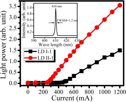
With 20kHz 500ns pulses, the output spectrum at 550mA current injection peaked at 410nm wavelength with 1.2nm full-width at half maximum (FWHM). The laser diode with u-GaN upper waveguide had a 229mA (3.8kA/cm2) laser threshold current, which compares with 425mA (7.1kA/cm2) for the reference device with more conventional structure (Figure 2). The light output power at 1200mA of the improved design also received a 137% boost from the u-GaN upper waveguide structure.

Figure 2: Light output power of LD I-1 (black) and LD II-1 (red, u-GaN upper WG) under pulsed current injection. Inset: optical spectrum of stimulated emission for reference LD I-1.
Although the 3.8kA/cm2 threshold is somewhat higher than the best achieved for III-N laser diodes (2.3kA/cm2), the researchers note that this was realized through a special ‘plasmonic’ GaN substrate from ultra-high doping in a high-pressure hydride vapor phase epitaxy (HVPE) growth process. The team suggests that their structure might be more economically feasible. Also, combining the u-GaN upper waveguide structure with plasmonic substrate might lead to further threshold reduction.
Undoped GaN Upper waveguide InGaN laser diode
https://doi.org/10.7567/JJAP.57.070307
The author Mike Cooke is a freelance technology journalist who has worked in the semiconductor and advanced technology sectors since 1997.


