- News
25 October 2017
Vertical gallium nitride p-n diode with 5.0kV breakdown performance
Hosei University and Sciocs Company Ltd in Japan have presented a vertical gallium nitride (GaN) p-n diode with a breakdown voltage (VB) of 5.0kV [Hiroshi Ohta et al, International Conference on Solid State Devices and Materials, Sendai, Japan, 22 September 2017, session N-6-02]. The team comments: “This value is the highest among so-far reported VB of the vertical structure GaN p-n diodes.”
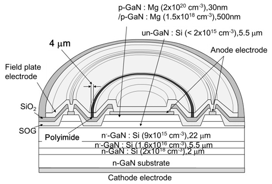
The device used a guard ring and resistor structure to reduce the potential at the edges of top contact where fields tend to crowd and become critical, causing breakdown.

Figure 1: Schematic of GaN p-n diode with guard-ring structure.
The material for the structure was grown by metal-organic vapor phase epitaxy. The substrate was free-standing GaN created using void-assisted separation – the threading dislocation density was less than 3x10⁶/cm2. Thermal annealing at 850°C for 30 minutes activated the magnesium p-type doping by removing hydrogen.
The resistor between the guard ring and central portion of the p-contact consisted of 4μm-wide Hitachi Chemical Co Ltd HD8820 photosensive polyimide, patterned and then cured at 350°C for 30 minutes. The circular palladium ohmic electrode had a diameter of 60μm.
The specific on-resistance of the device was 1.25mΩ-cm2 at 5V forward bias. This was close to the value for a circular p-n diode without guard-ring structure. Reverse bias with the guard-ring structure increased the breakdown to 5.0kV, about 200V greater than the 4.8kV value found for the diode without. Baliga’s figure of merit with guard-ring structure (VB2/Ron) was 20GW/cm2.

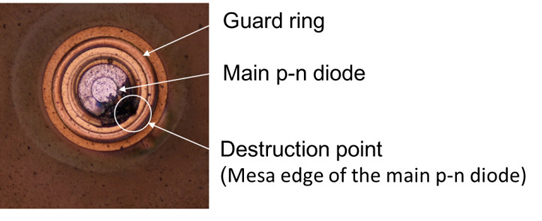
Figure 2: Surface destruction after breakdown.
The site of the breakdown (Figure 2) was found to be the edge of the main ohmic contact and not the guard ring, suggesting that the polyimide resistor had successfully kept the voltage of the guard-ring below its breakdown value, while not impacting the on-resistance. The researchers hope to increase the breakdown further by optimizing the resistor structure between the ohmic contact and guard ring.
GaN Vertical GaN p-n diode GaN
The author Mike Cooke is a freelance technology journalist who has worked in the semiconductor and advanced technology sectors since 1997.


