- News
8 September 2016
Indium gallium arsenide laser diode on exact germanium-on-silicon substrate
Researchers in Russia have developed an indium gallium arsenide (InGaAs) quantum well laser diode on (001) germanium-on-silicon 'virtual substrate' without offcut angle [V. Ya. Aleshkin et al, Appl. Phys. Lett., vol109, p061111, 2016]. Continuous-wave lasing with an emission wavelength of 941nm was possible at cryogenic temperatures of 77K. Room-temperature lasing at 992nm wavelength was restricted to pulsed mode.
The researchers hope that in future they will be able to extend the wavelength into the greater than 1.1μm (>1100nm) transparency range needed for use in conjunction with silicon waveguides. "It is assumed that the increase of the indium content in the InGaAs QW with an appropriate correction of the QW width could be a possible solution," the team writes.
Normally III-V materials such as InGaAs on (001)-oriented silicon (Si) are grown with a significant offcut angle of 4-6° to avoid the formation of anti-phase boundaries (APBs), which is a problem for polar materials deposited on non-polar substrates.
However, offcut angles complicate integration with silicon electronics and photonics. In addition, germanium (Ge) buffers are often used to accommodate lattice mismatching of III-V heterostructures with Si, but Ge on offcut Si is generally of low quality. Finally, offcut substrates lead to difficulty when cleaving the final devices into laser bars to give high-quality mirror facets.
The team from Institute for Physics of Microstructures of the Russian Academy of Sciences, Lobachevsky State University of Nizhny Novgorod, and FGUE 'Salut' produced their Ge/Si 'virtual substrate' by solid-source molecular beam epitaxy (SS-MBE). The n-Si substrate had a (001) crystal orientation with offcut angle less than 0.5°. A two-step process was used, involving deposition of 50nm Ge at 275°C and then the remainder at 600°C. The thin-layer growth allows strain relaxation through misfit dislocations. The higher-temperature growth gives better crystal quality material in the thicker layer. Further improvement was achieved with short-time cycle annealing. The annealing was found to reduce threading dislocation densities from 3x-4x10⁸/cm2 to ~107/cm2.
Table 1. Parameters of A3B5/Ge/Si(001) laser structure.
| Thickness (nm) | Doping (/cm3) | Remark | |
| Si(001) substrate (upper part) | . . . | Virtual substrate | |
| Ge | ~1000 | . . . | |
| AlAs/GaAs/AlAs | 10/50/10 | . . . | Planarizing buffer |
| GaAs:Si | 2500 | 2x10¹⁸ | Main buffer and n-contact |
| Al0.3Ga0.7As:Si | 1000 | 5x10¹⁷ | Bottom waveguide layer |
| GaAs | 340 | . . . | Active region with multiple InGaAs QWs |
| In0.17Ga0.83As QW | 10 | . . . | |
| GaAs | 50 | . . . | |
| In0.17Ga0.83As QW | 10 | . . . | |
| GaAs | 50 | . . . | |
| In0.17Ga0.83As QW | 10 | . . . | |
| GaAs | 170 | . . . | |
| GaAs:C | 170 | 3x10¹⁶ | |
| Al0.3Ga0.7As:C | 1000 | 5x10¹⁷ | Top waveguide layer |
| GaAs:C | 500 | 2x10¹⁹ | p-contact |
The III-V (A3B5) epitaxy involved metal-organic chemical vapor deposition (MOCVD) – see Table 1. In the initial planarizing buffer, two aluminium arsenide (AlAs) inserts were used to reduce GaAs-Ge interdiffusion and to filter out defects. The AlAs layer also reduced surface roughness by a factor of two.
There were some anti-phase boundaries (APBs) present due to the use of a substrate with near-zero offcut angle. The APB density in the buffer layer was around 0.6/μm. After the whole structure was grown the density was 0.3/μm. The researchers comment: "These values of the APB density are significantly smaller than the typical ones obtained during growth of polar materials on the exactly oriented non-polar Si(001) substrates. We believe that the influence of the APBs is not the main critical factor affecting the optical properties of the grown A3B5/Ge/Si(001) structure."

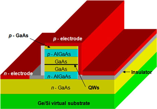
Figure 1. Schematic view of laser diode with planar ohmic contacts.
Laser diodes (Figure 1) were fabricated with the active region 20μm wide and 200μm wide planar ohmic contacts of gold-germanium-nickel-gold (n-type) and chromium gold (p-type). The substrate was thinned to 80μm. The material was cleaved into 2.7mm-long bars with mirror facets.

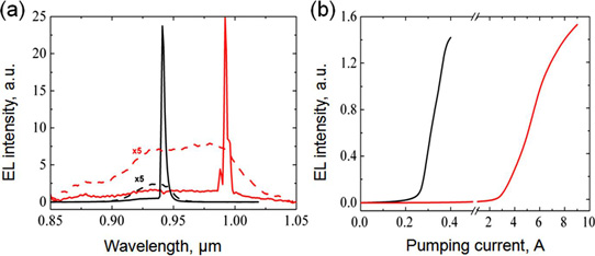
Figure 2. (a) Electroluminescence spectra at sub-threshold (dashed lines) and above threshold (solid lines). Black lines correspond to 77K, red ones to room temperature. For 77K (300K), pumping current density for subthreshold spectra was approximately 370A/cm2 (3.7kA/cm2); and for above threshold spectra 550A/cm2 (5.6kA/cm2). (b) Power-current characteristics of same laser diode.
Under electric current injection at 77K (Figure 2), the 941nm-wavelength emission peak narrowed from 30nm below threshold to less than 1nm above. Room-temperature (300K) 992nm emission was 95nm wide below threshold and narrowed to less than 1nm above. The threshold for lasing at 77K was 463A/cm2, low enough for continuous-wave operation. At 300K, only pulsed operation was possible with ~5.5kA/cm2 threshold.
InGaAs Laser diodes III-Vs-on-Si
http://dx.doi.org/10.1063/1.4961059
The author Mike Cooke is a freelance technology journalist who has worked in the semiconductor and advanced technology sectors since 1997.


