- News
27 September 2016
Integrating InGaAs well in ridges on 300mm silicon
Imec and Ghent University in Belgium have used aspect ratio trapping (ART) techniques to produce indium gallium arsenide (InGaAs) multiple quantum wells (MQWs) on 300mm-diameter silicon in a ridge format that could be used in future laser diodes [B. Kunert et al, Appl. Phys. Lett., vol109, p091101, 2016].
The work could lead to better integration of III-V light emitters and detectors into the developing silicon photonics industry that uses micron-scale waveguides to manipulate optical communications signals in the infrared. In particular, emitters and detectors are the vital interface between silicon electronics and optical systems.
At present, integration of emitters tends to be carried out using complex, expensive wafer- or chip-bonding, or through fiber connections from external sources. Direct integration of III-V materials on silicon should reduce process complexity and cost, but lattice mismatching reduces material quality and reduces the possibilities for efficient light emission, particularly for lasers.
ART techniques have been developed to reduce defect density in III-V structures on silicon and imec has used ART in its work on high-mobility transistors with a view to future high-speed/low-power electronics.
The imec/Ghent team now reports: "Despite the narrow trench dimension, the grown out III/V ridge has reached a volume suitable for wave guidance." The researchers add that they are investigating "optimized nano ridge structures with an increased GaAs volume and a confining InGaP cap layer to reduce carrier losses due to surface recombination". They expect realization of first nano ridge laser diodes using such techniques in the near future.
The III-V ridges were grown by metal-organic vapor phase epitaxy (MOVPE) on 300mm-diameter silicon with exact (001) crystal orientation. The trenches were provided by a shallow trench isolation (STI) process used in mainstream silicon electronics. The trenches were 10μm long and had varying widths. Trenches of the same width were arranged in 600μmx600μm fields. The trench areas were around 10% of the field. V-facets with (111) surfaces were formed by wet etching the silicon in the trench with tetramethylammonium hydroxide.
The GaAs deposition started with nucleation at 360°C using a triethyl-gallium precursor. The main growth inside and outside the trench was carried out at 580°C with trimethyl-gallium precursor. InGaAs layers for the quantum wells were also grown at 580°C.
The low-temperature nucleation/seeding was used to encourage two-dimensional growth, avoiding planar defects (stacking fault, twins, . , ,). The high-temperature growth gives a higher-quality GaAs crystal with misfit defect nucleation and threading dislocation gliding for full strain relaxation. Defects are trapped by the silicon dioxide trench walls. The researchers comment: "No indication of any misfit and threading dislocations was found above the STI level or close to the MQW region. Only three planar defects such as micro twins are visible in a 5.5μm-long transverse section."
The researchers comment: "It is of key importance to avoid the formation of stacking faults and twins from the beginning by an optimized seed layer and sufficient pre-cleaning of the Si surface, whereas the nucleation of misfit- and threading dislocations should be initiated as deep as possible in the trench, close to the Si surface, to benefit from a high aspect ratio."
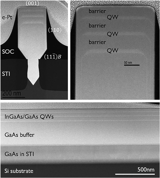
The GaAs above the trench grew in a box-shape cross-section. The boxes were rectangular for both narrow and wide trenches. The researchers report that "the ridge courses are very straight and uniform with flat surfaces in all directions, which is essential for realizing a waveguide with low light scattering losses."

Figure 1: High-angle annular dark-field (HAADF) scanning transmission electron microscopy (STEM) of box-shaped GaAs ridge with three InGaAs QWs. Top left: cross-section of full ridge. Top right: higher magnification of QW region. Bottom: transverse section along trench. The GaAs inside STI shows slightly different contrast because some STI oxide was cut out during sample preparation.
Reciprocal-space mapping using x-rays indicated that the GaAs ridges were fully relaxed. The InGaAs quantum wells were grown pseudomorphically on the GaAs buffer with ~19% indium content (Figure 1). From bottom to top, the well thicknesses were 9.9nm, 8.9nm, and 7.7nm. The periods of time for growth of the three wells was the same, as also for the three GaAs barrier layers. Although the growth is mainly on the top surface, there is some side-wall deposition.
The researchers comment: "Side-wall deposition leads to a very good lateral carrier confinement, reducing non-radiative recombination channels at the QW side surfaces and is therefore desirable. Especially the evolving decrease in InGaAs thickness at the lateral ends of the QWs will lead to higher quantized electronic states, which induces an injection and repulsing of electrons and holes in the InGaAs layer at the box edges towards the centered QW region with constant layer thickness and lower energetic states. The InGaAs layer of less than 2nm thickness on the {110} side walls is too thin to hold bonded states with an efficient radiative recombination rate."
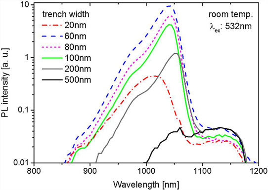
In photoluminescence (PL, Figure 2), a peak was seen between 1000nm and 1050nm, except for the very widest trench of 500nm. The photo-emission from the QWs was orders of magnitude higher than from the silicon substrate, which was centered around 1140nm. Some of the spectra show a shoulder around 980nm, which could be due to higher quantized states of the wells. The brightest peak was for 60nm-wide trenches. However, comparisons are complicated by factors such as ridge volume, carrier density, surface states, and so on.

Figure 2: Room-temperature PL spectra from different trench widths in log-scale.
The team comments: "Although it is difficult to judge about the overall impact of these uncertainties, it is very likely that the decrease in PL intensity towards wide trenches is linked to an increase in TD density. The aspect ratio of trenches wider than 100nm is quite low, leading to an insufficient defect trapping. Hence, the remaining defect density in the ridge material of wider trenches could cause high carrier losses. The intensity decline towards narrow trenches could be related to a disproportional rise in ridge surface area or less pump light absorption."
The differences in peak position are likely due to changes in indium content and/or QW width. The photoluminescence linewidth was 38meV for material grown from 100nm-wide trenches.
InGaAs MQWs InGaAs Laser diodes
http://dx.doi.org/10.1063/1.4961936
The author Mike Cooke is a freelance technology journalist who has worked in the semiconductor and advanced technology sectors since 1997.


