- News
4 March 2016
Vertical epitaxial heterostructure GaAs optical transducers
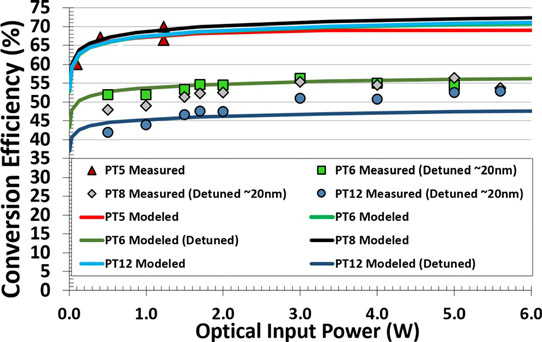
Researchers in Canada claim the highest reported optical-to-electric power conversion of more than 65% (Figure 1) for a 150W/cm2 (~1500 suns) tuned narrow spectrum input from high-powered laser diodes [S. Fafard et al, Appl. Phys. Lett., vol108, p071101, 2016]. Multi-junction concentrated photovoltaic cells have achieved 46% conversion from the broad solar spectrum.

Figure 1: Power dependence of measured and modeled optical-to-electrical conversion efficiency for GaAs phototransducer heterostructures engineered with the VEHSA design. When input wavelength is tuned to peak response, the efficiency approaches 70%.
The optical transducers were based on a vertical epitaxial heterostructure architecture (VEHSA) design of a number of monolithically integrated thin n-p gallium arsenide (GaAs) junctions. The team - consisting of researchers from Université de Sherbrooke, Azastra Opto Inc, and University of Ottawa - sees potential for microelectronic hybrid components and biomedical applications. Such uses could benefit from output voltages in the 5-12V range, enabled by employing stacks of junctions.
The researchers comment: "These features are sought after in order to enable more compact, electrically isolated, or long-lasting power sources. Such isolated power supplies are beneficial for regulating more securely microelectronic circuits in many telecommunication, utilities, sensor, and automotive systems, or for controlling more safely neuro-stimulating or biomedical devices."
Metal-organic chemical vapor deposition (MOCVD) was used to produce heterostructures on 150mm-diameter zinc-doped p-GaAs substrates. Stacks of GaAs n-p junctions were grown on a lattice-matched gallium indium phosphide (GaInP) p-type back surface field. An n-type window layer of lattice-matched GaInP completed the structure.
The n-p junctions were generally connected by high-peak-current p++-/n++-type aluminium gallium arsenide (AlGaAs) tunnel junctions developed by some of the team. The more usual tunnel junction for such connections in concentrated photovoltaic (CPV) devices consists of n++-GaInP/p++-AlGaAs. The five-junction (PT5) devices did not use the p++-AlGaAs/n++-AlGaAs tunnel junction. PT5 devices were also limited to less than 1W optical input.
The n-GaAs part of the n-p junctions was around 100nm or thinner. The p-GaAs side of the junction was varied in thickness. The 12-junction devices had p-type layers as thin as 44nm.
The heterostructures were designed using a combination of preliminary experiments – photoluminescence and photo-electrical – and simulations. The aim was, naturally, for close to 100% conversion across the structure.
Silver gridlines formed an ohmic contact with an n++-GaAs layer on the n-GaInP window.
The devices were designed to operate at longer than 700nm input radiation. The window layer was transparent to this light and the absorption was expected to be important only in the GaAs n-p layers with optimal performance between 805nm and 845nm. An 830nm-wavelength anti-reflection coating was used.

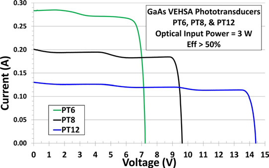
Figure 2: Measured current-voltage curves at 20°C with input at 825nm.
The number of n-p junctions affects the maximum output voltage, with 6.0V for five junctions and 14.6V for 12 (Figure 2). These give about 1.2V open-circuit voltage (Voc) per junction.
The researchers comment: "Our test setup with high-power laser diodes having fixed ouput wavelengths did not allow us at this time to complete the measurements under fully tuned conditions for all the VEHSA designs. Still, from the modeled and measured optoelectronic properties, we can deduce that the thin individual n/p junctions are each generating ~1.2V of Voc when illuminated with an average intensity of a few W/cm2. We can also deduce that the voltage of the thinner n/p junction can be higher than for the thicker heterostructures by at least ~20mV."
GaAs phototransducer GaAs MOCVD
http://dx.doi.org/10.1063/1.4941240
The author Mike Cooke is a freelance technology journalist who has worked in the semiconductor and advanced technology sectors since 1997.


