- News
8 January 2016
Going beyond gallium nitride transistor state-of-the-art performance
The imec research center in Belgium claims beyond state-of-the-art performance for a p-type gallium nitride (p-GaN) high-electron-mobility transistor (HEMT) on silicon operating in enhancement-mode (normally-off). The threshold voltage was +2V. Low on-resistance of 7Ω-mm enabled high drive current of 0.4A/mm at 10V drain bias. imec presented its results at the IEEE International Electron Devices Meeting in Washington DC, USA (8 December 2015) in sessions 16.2 and 35.4. imec claims that the p-GaN HEMT outperforms metal-insulator-semiconductor (MISHEMT) counterparts.

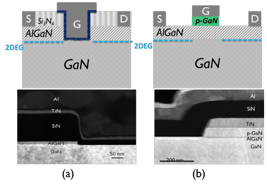
Figure 1: Schematic cross section (upper figures) and transmission electron micrographs (TEMs) of gate region (lower figures) of (a) recessed-gate MISHEMT and (b) p-GaN HEMT.
imec has been working on the p-GaN HEMT structure (Figure 1) for some time [Forward-bias gate breakdown in HEMTs with enhancement-mode p-GaN gate]. Normally-off/enhancement-mode operation is preferred for power efficiency and fail safety. Conventional GaN HEMTs, produced without special measures such as fluoride plasma treatment of the gate region, tend to be depletion-mode/normally-on. Producing GaN devices on silicon should lead to production cost savings, but device performance can be impacted by crystal defects arising from the larger lattice mismatch, compared with silicon carbide (SiC) or free-standing/bulk GaN substrates.
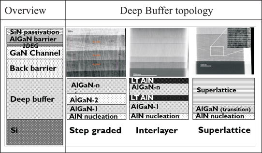
One team of imec researchers focused on improving the interface between the 200mm-diameter substrate and the overlying GaN buffer with the aim of reducing dispersion/current collapse. Dispersion occurs in pulse-mode/switching operation. One cause of this is trap states in the buffer layer that adversely affect performance compared with DC characterization. Three types of high-voltage buffer/silicon interface were compared: step-graded, low-temperature AlN interlayer, and superlattice (Figure 2). Using a 'design of experiments' methodology, the researchers conclude that "a superlattice buffer can achieve simultaneously low dispersion and leakage under negative bulk bias".

Figure 2: Schematic overview of AlGaN/GaN buffer and constituent parts. Schemes of three different deep buffer topologies are shown and illustrated with TEM cross sections of epi buffers.
In their optimization efforts, the team aimed at low dispersion/current collapse, leakage and breakdown voltage over a wide temperature range and bias conditions. The researchers also optimized the epitaxy process for the p-GaN part of the gate stack on top of the aluminium gallium nitride (AlGaN) barrier layer.
imec says that it is working towards industrialization and is offering a complete 200mm CMOS-compatible 200V GaN process line that features excellent specs on enhancement-mode devices.
The author Mike Cooke is a freelance technology journalist who has worked in the semiconductor and advanced technology sectors since 1997.


