- News
27 January 2016
Fujitsu develops GaN power amplifier with record output for W-band wireless transmission
Japan's Fujitsu Ltd and Fujitsu Laboratories Ltd have developed a gallium nitride (GaN) high-electron-mobility transistor (HEMT) power amplifier with record output performance for W-band (75-110GHz) transmission by using a proprietary structure (Figure 1). This can be used in a high-capacity wireless network with coverage over a radius of several kilometers.
 Figure 1: Chip containing the new W-band GaN-HEMT power amplifier.
Compared to today's mobile phones, which use frequencies in the 0.8-2.0GHz range, the W-band uses a frequency band more than 50 times as broad with 50 times the speed, making it is well suited to high-capacity wireless communications. High-frequency wireless communications using W-band frequencies are drawing increasing interest, both as a way to temporarily set up high-capacity communications channels for handling special events where large numbers of people gather, or for responding to disasters, and also as a way to bring communications to remote areas where fiber-optic cables are difficult to lay.
However, to transmit wireless signals over a distance of several kilometers, the transmission antenna needs a power amplifier capable of a high output, on the order of several watts. Existing power amplifiers for high-frequency transmissions in the millimeter-wave band (30-300GHz), built using gallium arsenide or CMOS semiconductors, are limited by their operating voltage to an output of about 0.1W, and it has not been possible to increase this.
GaN-HEMT power amplifiers have achieved high output performance in the microwave range (3-30GHz), but the problem up until now was that their output performance declined in the W-band range.
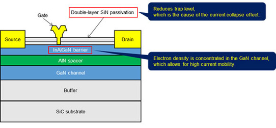
To design a power amplifier with high output performance, Fujitsu developed a GaN-HEMT device with a unique structure - presented at the 2015 IEEE International Electron Devices Meeting (IEDM) in December - capable of increasing output in the millimeter band (Figure 2).
This uses a layer of indium aluminium gallium nitride (InAlGaN) and a double-layer silicon nitride (SiN) passivation film to increase current density by a factor of about 1.4, resulting in 3.0W of output power from a transistor per mm of gate width, at a high frequency of 100GHz. In developing this transistor, Fujitsu collaborated with the Tokyo Institute of Technology's professor Yasuyuki Miyamoto in developing device simulation technology.

Figure 2: Cross-sectional diagram of the GaN-HEMT device.
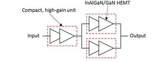
Fujitsu precisely measured and modeled the characteristics of the GaN-HEMT during high-frequency operation. Based on that, a circuit was designed where pairs of GaN-HEMTs were grouped together into compact, high-gain units with low power loss. In order to maximize the power from these units, the GaN-HEMTs were connected in a series by the inter-stage circuit where the signal lines and the device layouts were carefully laid out.
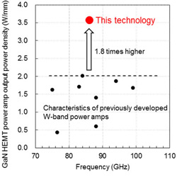
Using a model of these compact, high-gain units, Fujitsu conducted simulations to optimize the distributor and combiner matching circuits between the units, and their layouts and signal lines, resulting in a high-amplitude power amplifier (Figure 3). A prototype power amplifier had amplitude that multiplied its input by a factor of 80, producing 1.15W of output power. Power output per transistor (a measure of power-amplifier performance) was 3.6W per mm of gate width (claimed to be a record).

Figure 3: The compact, high-gain circuit that was used.
Evaluation of the new power amplifier confirmed that it achieved a 1.8 times increase in output over previous W-band power amplifiers (Figure 4). This translates to an improvement of over 30% in transmission range for high-speed wireless communications networks operating at speeds of several gigabits per second.
 Figure 4: Performance index of GaN-HEMT power amplifiers.
Fujitsu plans to apply this power amplifier technology to high-capacity long-range wireless communications, and to implement high-speed wireless communications systems that can be used for high-expediency temporary communications infrastructure for use during special events and when fiber-optic links have been broken in the event of disasters.
Some the research was conducted as part of a project of Japan's National Institute of Information and Communications Technology (NICT) on 'Agile Deployment Capability of Highly Resilient Optical and Radio Seamless Communication Systems'. Details were presented at IEEE Topical Conference on RF/Microwave Power Amplifiers for Wireless and Radio Applications (PAWR2016) in Austin, Texas (24-27 January).


