- News
2 December 2016
Multi-functional metamorphic buffer for InAs QW laser diodes on InP
Yale University and University of Illinois at Urbana-Champaign in the USA have developed a multi-functional metamorphic buffer (MFMB) for indium phosphide (InP) substrates that acts both as a bridge between lattice constants and optical confinement for laser diodes (LDs) [Daehwan Jung et al, Appl. Phys. Lett., vol109, p211101, 2016]. The researchers have demonstrated the concept for 2.5μm short-wavelength infrared (SWIR, 1.4-3μm) devices with lasing up to room temperature (RT) in pulsed mode.
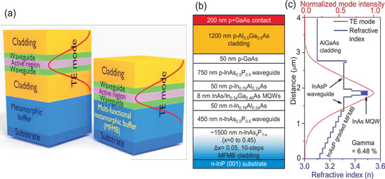
Usually the buffer layer that is used to bridge lattice mismatching is separate from the cladding layers that are used to provide optical confinement in laser diode structures. This increases the amount of material needed to be grown epitaxially, adding to processing times and costs. The MFMB was used to both bridge the substrate-laser lattice structures and provide graded-index cladding for optical confinement.
The team hopes that the technique could open up the range of semiconductor laser devices, allowing wavelength 'gaps' to be accessed efficiently. The 2-3μm range is one such gap. While other technologies – InP-based laser diodes or quantum cascade lasers (QCLs) from opposite ends – can be stretched into this gap, the result is usually suboptimal.
Gallium antimonide (GaSb) is often used as a substrate for SWIR LDs, but the material has lower thermal conductivity and immature commercial processing infrastructure compared with InP built up through extensive 1.55μm laser diode telecoms (i.e. fiber-optic) applications.
The researchers comment that the approach could be extended to devices on gallium arsenide (GaAs) or silicon (Si): "More generally, the MFMB concept may enable a new class of laser diodes for many applications such as GaAs-based mid-IR lasers or photonic integrated circuits (PICs) on Si," they write.
The Yale/Urbana-Champaign MFMB provided the bottom cladding for the laser diode, while the top cladding came from low-index p-AlGaAs (Figure 1). The asymmetric-index InAsP waveguide structure was designed to center the fundamental transverse-electric (TE) optical field on the active region of the device. The confinement factor in the nine compressively strained QWs was estimated at 6.8%.

Figure 1: (a) Schematic comparison of conventional laser diodes grown on metamorphic buffers and MFMB. (b) MFMB laser diode structure. (c) Optical TE mode intensity profile (red) and refractive index (blue) in graded InAsP MFMB laser diode.
Compressive strain leads to highly TE-polarized emission from the QWs. The strain-balancing of the QW region was achieved by performing photoluminescence studies with 8nm InAs QWs and 6.1nm In0.54Ga0.46As barriers. The barriers were under tensile strain. The light-emission performance of this structure was much better than using 15nm InAs0.5P0.5 unstrained barriers. In fact, a single InAs QW outperformed 4 InAs QWs with unstrained barriers. Bright-field transmission electron microscopy showed the strain-balanced structure to be 'free' of misfit dislocations, unlike the unbalanced QWs.
The MFMB laser material was grown on InP by molecular beam epitaxy (MBE). The 10μm-wide laser ridge fabrication consisted of freon and inductively coupled plasma (ICP) etches. Electrical isolation was provided by 300nm silicon dioxide.
Contact pad regions were opened in the silicon dioxide layer and titanium/aluminium/gold p-contact metals applied. The back-side germanium/gold/nickel/gold n-contact was applied after lapping the laser material to the thickness range 150-200μm. Metal deposition was followed by annealing/alloying at 405°C for 5 minutes.
The material was cleaved into 1mm-long laser bars and mounted on a copper block with indium paste. The assembly was placed in a cryostat.
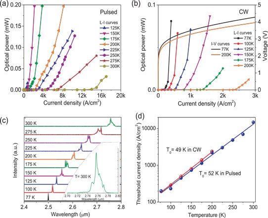
At 77K, the continuous-wave emission was at 2.50μm (0.5eV) with 108nm full-width at half maximum (FWHM) at a low current density of 120A/cm2. The emission wavelength was consistent with the calculated energy of the QW ground-state electron-hole transition. By 250A/cm2 current density, the FWHM fell dramatically to 2nm with much increased peak intensity, indicating laser behavior.
Light output power versus current curves indicate laser thresholds up to 300K for pulsed operation and 200K for continuous wave (Figure 2). "While the MFMB structure enables lasing by providing optical mode confinement and low threading dislocation density, the strain-balanced MQW active region improves the laser gain, enabling RT operation," the researchers comment.

Figure 2: (a) Temperature-dependent pulsed-mode light output power versus current. (b) CW mode light output power and voltage versus current. (c) Pulsed-mode lasing spectra. Inset: 300K close-up. (d) Threshold current density versus temperature in CW (red) and pulsed mode (blue). Solid lines: semi-log fit.
The differential quantum efficiency was estimated at 4.6% and 0.13% for continuous-wave operation at 77K and 200K, respectively. Pulse-mode operation also saw a strong fall in differential quantum efficiency with temperature, except around 250K.
The emission wavelength red-shifted with increasing temperature, in line with an expected narrowing of the bandgap of the InAs QWs. At 300K/room temperature, the pulse-mode emission wavelength was 2.76μm.
The increase and relatively high threshold currents in both pulsed and continuous modes causes the researchers to comment: "Although the MFMB concept has enabled the longest-wavelength room-temperature emission for a type-I laser diode on InP, the threshold current density is still relatively high at this early stage. Improvements in laser performance can be obtained by optimizing the growth conditions and carrier confinement for the InAs MQW layers to increase the internal quantum efficiency. Optimization of the p-type doping profile will also be necessary to decrease the voltage drop across the device, diminish parasitic absorption, and improve the device temperature performance."
The team also suggests that further enhancements for lower thresholds could include graded-index top cladding based on AlGaAs and facet coating to adjust reflectivity at the ends of the cavity.
Multi-functional metamorphic buffer InP substrates
http://dx.doi.org/10.1063/1.4968560
The author Mike Cooke is a freelance technology journalist who has worked in the semiconductor and advanced technology sectors since 1997.


