- News
13 October 2015
Claiming record 4.7kV breakdown for gallium nitride p-n diodes
Researchers in Japan have claimed record breakdown voltage combined with low on-resistance for vertical gallium nitride (GaN) p-n diodes fabricated on free-standing GaN substrates [Hiroshi Ohta et al, IEEE Electron Device Letters, published online 22 September 2015]. This was achieved using a triple-drift-layer structure. In particular, the layer next to the p-type GaN was very lightly doped so that the peak field near the p-n junction was suppressed, allowing higher voltages to be sustained. A second moderately doped layer reduced on-resistance.
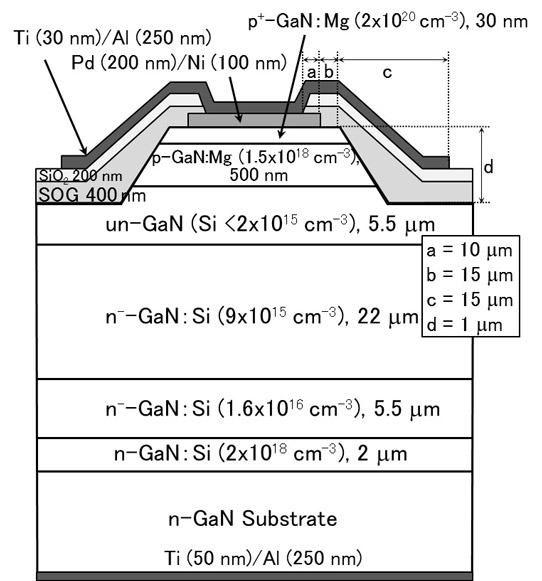
The research team came from Hosei University, Quantum Spread Co Ltd, and Hitachi Metal subsidary Sciocs Co Ltd. They used 2-inch free-standing GaN substrate for the devices (Figure 1). These substrates were produced by void-assisted separation, resulting in a threading dislocation density of less than 3x10⁶/cm2.

Figure 1: Schematic cross sections of the GaN p-n junction diodes with the triple drift layers and the FP structure.
The device material was grown using metal-organic vapor phase epitaxy. The researchers used specially designed diluted silane gas lines to achieve the very low silicon doping for the lightly doped n--GaN layers. The researchers comment: "By reducing the doping concentration underneath the p-GaN layer, the peak electric field at the p-n interface can be suppressed under negatively biased conditions."
The silicon doping profile was confirmed by secondary-ion mass spectroscopy, but the limit of the measurement was around 9x10¹⁵/cm3. The researchers believe that the actual doping concentration in the most lightly silicon-doped n--GaN layer could be less than this.
The material was annealed at 850°C for 30 minutes before device fabrication to activate the magnesium doping of the p-GaN layers.
The device included a field-plate (FP) structure on sputtered silicon dioxide/spin-on-glass (SiO2/SOG) insulator/passivation for the p-type ohmic contact to the p-GaN layer.
A triple-drift-layer device with 100μm-diameter circular p-electrode achieved an on-resistance (Ron) as low as 1.7mΩ-cm2. A comparison device with double drift layer (2μm undoped and 22μm 1.1 x 1016 cm3 silicon doping) had a lower on-resistance of 1.4mΩ-cm2. The turn-on voltage was around 3.1V.
The researchers comment: "These low Ron's were brought by high-quality epitaxial layers grown on the GaN substrates with low dislocation density. The high-quality layers enhances photon-recycling effect which increases conductive holes from deep Mg acceptors excited by high-density photons generated through electron-hole-pair recombination at the p-n junction."
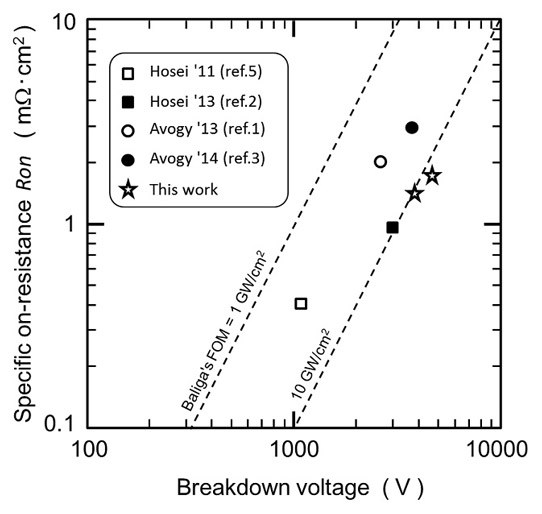
Triple-drift-layer devices with electrode diameters of 60μm and 200μm achieved reverse breakdown voltages as high as 4.7kV, which is 1kV higher than a single-drift-layer diode reported in 2014. Recently, US-based Avogy reported a diode on bulk GaN with breakdown exceeding 4kV. Ohta et al's double-drift-layer structure achieved 3.8kV breakdown.
The researchers comment that it might be possible to obtain similar or higher breakdown voltage from a single undoped GaN thicker layer, but the Ron would increase significantly because of lower electron carrier densities under forward bias. "Hence, the particular drift layer of this study was shown to be effective in raising the total performance of GaN p-n diodes," they add.

Figure 2: Relationship between the specific on-resistance and breakdown voltage of the GaN p-n junction diodes fabricated by Ohta et al with previously reported results.
The Baliga figure of merit (FOMs) – (breakdown voltage)2/Ron – was 13GW/cm2, "the best values ever reported among those achieved by GaN p-n junction diodes on free-standing GaN substrates," according to the team. GaN devices have previously achieved Baliga FOMs an order of magnitude larger than for silicon carbide Schottky-barrier diodes.
The breakdown for the GaN p-n diodes occurred at the mesa or field-plate edge, suggesting that improvements in insulation and field-plate fabrication could increase breakdown performance.
GaN p-n diodes GaN Free-standing GaN substrates
http://ieeexplore.ieee.org/xpl/abstractAuthors
The author Mike Cooke is a freelance technology journalist who has worked in the semiconductor and advanced technology sectors since 1997.


