- News
18 May 2015
Bevel junction termination extension for silicon carbide high voltage
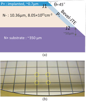
North Carolina State University in the USA has developed a new edge termination technique for 4H polytype silicon carbide (4H-SiC) high-voltage devices [Woongje Sung et al, IEEE Electron Device Letters, published online 29 April 2015]. The technique involves beveling the device and creating a junction termination extension (JTE) with implanted aluminium doping (Figure 1). Edge terminations are designed to avoid field crowding effects that cause premature breakdown.

Figure 1: (a) Schematic cross section of a PiN rectifier with the Bevel-JTE. Over-diced area into the substrate is used for the final dicing, (b) wafer image after bevel dicing. Corners of the Bevel-JTE are indicated by dashed circles.
The researchers used an angled dicing blade to create the bevel. Angles between 30° and 90° could be achieved easily. The angle and feed speed were chosen to reduce surface roughness and chipping.
The doping of the JTE needs to be adjusted to avoid locating the high field at either the bottom of the pn junction (high doping) or at the main junction (low doping). Both extremes result in lowered breakdown voltage. The high doping condition also increases leakage currents.
A range of 4H-SiC p-i-n rectifiers were fabricated with chip size 4mmx4mm. The top p+ layer was doped with aluminium implantation of total dose 2x10¹⁵/cm2 at 300keV.
The bevel-JTE was formed using orthogonal bevel dicing and ion implantation. The dicing blade was V-shaped with a 45° angle. Damage from the sawing step was removed with a 0.3μm reactive ion etch. Doping activation was achieved with annealing at 1800°C for 5 minutes. Leakage current could be reduced by rapid thermal annealing (RTA) at 1000°C for 1 minute in laughing gas, more soberly known as nitrous oxide (N2O).
The researchers achieved maximum breakdown voltage of 1600V with an anode current density of 1mA/cm2. The breakdown was 95% of the maximum theoretical value for a one-dimensional model. Bevel implant doses in the range 1-2x10¹³/cm2 gave the maximum breakdown. The breakdown was reduced to ~800V for 3x10¹³/cm2 dosage due to current leakage.
Comparison with simulation results suggest incomplete activation of the doping (~50%). The researchers suggest that the annealing may evaporate some of the dopant and create unintentional doping elsewhere in the structure. "This results in higher measured breakdown voltages than shown by simulation," the team adds.

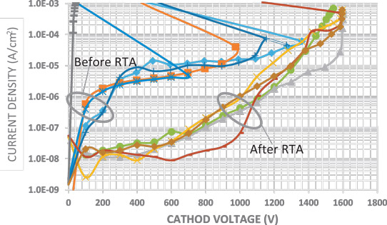
Figure 2: Effect of RTA on reducing leakage current. Reverse blocking characteristics before and after the RTA process on same dies implanted at 2×10¹³/cm2.
The RTA process reduced current leakage significantly (Figure 2). The researchers attribute the improvement to curing of implant-induced defects and damage, reducing the concentration of active carrier trapping centers.
The researchers comment: "Since the Bevel-JTE is fabricated with a dicing blade, it can be simply applied to any vertical device in SiC that has a drift layer of different thickness by adjusting the dicing depth. In fact, it is more attractive to use the Bevel-JTE structure for higher-voltage devices because a significantly large area of the wafer is occupied by edge termination structures using the conventional approaches."
The team estimates that the bevel-JTE is three times narrower than conventional approaches to edge termination. Also, the complexity and implant dose sensitivity is reduced. The researchers believe the technique can be used for other devices with different ranges of breakdown voltage.
http://ieeexplore.ieee.org/xpl/articleDetails.jsp?arnumber=7097678
The author Mike Cooke is a freelance technology journalist who has worked in the semiconductor and advanced technology sectors since 1997.


