- News
13 March 2015
First in-situ PL of growing InGaN/GaN MQW LED structure during MOCVD
In a collaboration with professor Dirk Rueter´s group at the University of Applied Sciences Ruhr West, in-situ metrology system maker LayTec AG of Berlin, Germany have achieved what is clamed to be the first quasi-continuous in-situ photoluminescence (PL) monitoring of InGaN/GaN multi-quantum-well (MQW) emission wavelength during metal-organic chemical vapour deposition (MOCVD) in an industrial-grade reactor at growth temperature (C. Prall et al, Journal of Crystal Growth 415 (2015), 1–6).
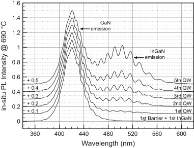
 In-situ spectra of a growing InGaN MQW structure (solid lines) at wafer temperature of 690°C. The spectra of the complete QWs were taken after growth of the subsequent GaN barrier layer.
It is well known that room-temperature wafer-based PL measurements – even at an early stage of the growth of the active region – provide an excellent forecast of the emission wavelength and emission intensity of resultant LED devices. In this latest collaborative work, a prototype in-situ PL system was used simultaneously with a LayTec Pyro 400 tool in a commercial multi-wafer MOCVD reactor at growth temperature. The study hence demonstrated accuracy of ±1.3nm (2σ) in the predicted wavelength range. The researchers conclude that the technique thus appears to be suitable for the closed-loop control of the emission wavelength of InGaN LEDs during growth.
The work has been supported by BMWi (German Federal Government) under grant KF3242801NT3.
www.sciencedirect.com/science/article/pii/S0022024814008380


