- News
18 June 2015
Indium surfactant for higher hole concentration in gallium nitride
University of California Santa Barbara (UCSB) in the USA has improved hole concentrations in p-type gallium nitride (p-GaN) by using indium as a surfactant in ammonia-based molecular beam epitaxy (NH3MBE) [Erin C. H. Kyle et al, Appl. Phys. Lett., vol106, p222103, 2015].
The difficulties in producing p-type magnesium (Mg) doping of GaN have hampered the production of efficient light-emitting devices. The Mg acceptors have an activation energy of ~200meV, which means that most of the acceptor atoms are not ionized at room temperature (300K ~ 26meV). In addition there are donor states (even in undoped GaN) that partially compensate for the holes released from the ionized acceptors. Nitrogen vacancy defects are thought to be one source of these compensating donor states. Hydrogen can also play a role in reducing p-GaN doping efficiency [see www.semiconductor-today.com/news_items/2015/jun/kopti_100615.shtml].
The 200nm-thick p-GaN layers were grown on Lumilog semi-insulating iron-doped GaN-on-sapphire templates. The MBE was performed in a Veeco 930 system with effusion cells as Ga, In and Mg sources. The nitrogen source was ammonia delivered through an unheated showerhead injector. Extreme nitrogen-rich conditions were used, with the ammonia/III ratio being more than 3700.
First the researchers studied the effect of increasing the indium surfactant flux on the hole concentration in 4.5x10¹⁹/cm3 Mg-doped GaN, created using 700°C MBE. The highest hole concentration came with an In flux of 5x10⁻⁸Torr beam equivalent pressure (BEP). The Ga flux was the same. The residual In concentration in the grown material was between 6.0x10¹⁹/cm3 and 1.3x10²⁰/cm3.
The effect of temperature was analyzed in growth with 5x10⁻⁸Torr In flux and 6x10¹⁹/cm3 Mg doping. The resistivity and hole concentration for 700°C growth were 0.59Ω-cm and 1.6x10¹⁸/cm3, respectively. The residual In concentration was 1x10²⁰/cm3.

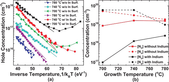
Figure 1: (a) Fit of temperature-dependent hole data for growth temperature series using charge balance equation. Ea0 fitted globally for all data sets; Ea calculated for each data set at each temperature. Data below 170K were not included in fit. (b) Fitted acceptor (NA) and donor (ND) concentrations for temperature-dependent data.
Temperature-dependent Hall measurements were used to disentangle the concentration of acceptor and donor impurities in the Mg-doped GaN with and without In surfactant (Figure 1). It was found that the surfactant mainly suppressed the compensating donor concentration. The analysis assumed that the ionization energy of the acceptors was 0.183eV (183meV) in the absence of ionized acceptors (Ea0). The lowest-temperature growth at 700°C gave the highest acceptor and lowest donor concentrations
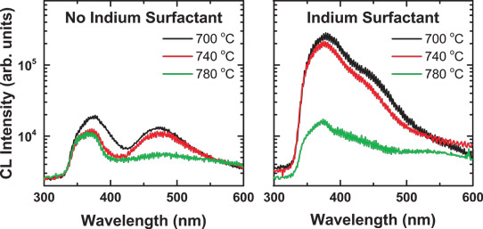
The use of indium surfactant also improved band-edge cathodoluminescence (CL) by about an order of magnitude for 700°C and 740°C p-GaN (Figure 2). The electron excitation voltage was 7kV with estimated 275nm penetration. Most of the luminescence was expected from the p-GaN since the iron-doped GaN template layer should give negligible intensity. Both samples showed similar levels of blue luminescence associated with optical transitions involving the Mg acceptor.

Figure 2: Cathodoluminescence spectra for growth temperature series.
The researchers comment: "The nitrogen vacancy is believed to contribute to the reduction in p-type conductivity in NH3MBE-grown films and may be the defect suppressed in this study. The nitrogen vacancy may also be forming complexes with Mg at higher growth temperatures, causing the ~6x reduction in acceptor concentration observed in our films. Hydrogen may also be forming complexes with Mg, but the decrease in acceptor concentration was greater than the total hydrogen concentration observed in the films."
p-GaN Ammonia-based molecular beam epitaxy GaN MBE
http://dx.doi.org/10.1063/1.4922216
The author Mike Cooke is a freelance technology journalist who has worked in the semiconductor and advanced technology sectors since 1997.


