- News
29 July 2015
Lowering threshold currents for m-plane III-nitride VCSELs
University of California Santa Barbara (UCSB) in the USA has reduced the threshold current density of its non-polar m-plane III-nitride vertical-cavity surface-emitting lasers (VCSELs) by a factor of five [J. T. Leonard et al, Appl. Phys. Lett., vol107, p011102, 2015].
The reduction is attributed to the use of a planar indium tin oxide (ITO) design, and the replacement of the plasma-enhanced chemical vapor deposition (PECVD) silicon nitride aperture by an aluminium (Al) ion implant process. The ion implant aperture also reduced the forward voltage by about 1V for given current density.
Longer-wavelength VCSELs using other III-V compound semiconductor materials benefit from structures with small active-region volume, short cavity length, circular beam profile, low beam divergence, and perpendicular emission from the substrate.
The UCSB team sees potential from similar properties for III-nitride devices for applications such as plastic optical fiber (POF) and free-space data communication. Single-mode operation could be useful in atomic clocks.
VCSELs can be formed into 2D arrays, which could lead to high-power-density ultraviolet III-nitride devices for pico-projectors, micro-displays, backlighting for small electronics, laser-based lighting, and bio-sensing.

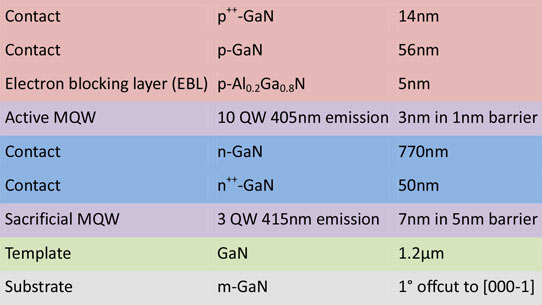
Figure 1: Epitaxial layer structure.
The use of the m-plane oriented III-nitride structures avoids performance degradation from the quantum-confined Stark effect and also benefits from lower transparency carrier and current densities, higher material gain, and anisotropic gain characteristics, compared with conventional c-plane structures.
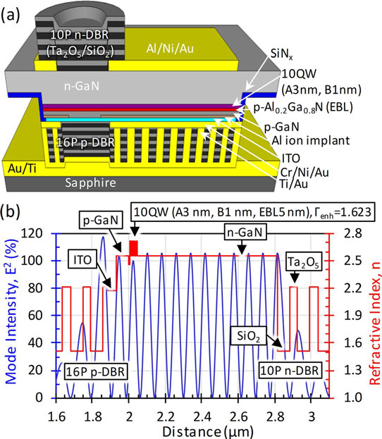
The epitaxial structure (Figure 1) was grown on Mitsubushi Chemical m-plane gallium nitride (GaN) using atmospheric-pressure metal-organic chemical vapor deposition (AP-MOCVD). After p-GaN activation, the VCSEL fabrication (Figure 2) began with etching of a 300nm mesa. The laser aperture was created using aluminium ion implantation (outsourced to Leonard Kroko Inc) with a titanium/gold hard mask. Next, a patterned 47nm ITO intra-cavity contact was deposited and silicon nitride was applied to the mesa sidewalls.

Figure 2: (a) Schematic of flip-chip non-polar VCSEL. (b) Cavity-mode intensity E2 (normalized to the peak in the active region) and refractive index profile of 10-period MQW.
A 16-period distributed Bragg reflector (DBR) was deposited on a chromium/nickel/gold stack on the p-side ITO. The DBR consisted of tantalum pentoxide and silicon dioxde layers with a 1/8-wavelength tantalum pentoxide spacer next to the ITO.
The silicon nitride on the mesa sidewalls was etched away from the region of the sacrificial indium gallium nitride (InGaN) multiple quantum well (MQW) to prepare for photo-electro-chemical (PEC) etching. Also, titanium/gold was applied as a conformal coating around the DBR to form the PEC cathode and p-contact pad for the VCSEL.
The structure was then flip-chip bonded at 200°C for 2 hours to a sapphire substrate with titanium/gold coating using a graphite compression fixture. The PEC was carried out to remove the substrate and sacrificial MQW, exposing the n-GaN contact layer. The PEC used potassium hydroxide solution and 405nm excitation from a laser diode.
The VCSEL was completed with deposition of an aluminium/nickel/gold n-contact and 10-period DBR.
The researchers increased the number of active QWs to 10, over 5 in previous work, in the hope of reducing the threshold current density from 89kA/cm2. The higher number of wells compensated for anomalous losses in the ITO contact layer. If the ITO losses could be reduced, lower numbers of wells would be more favorable, according to the researchers.

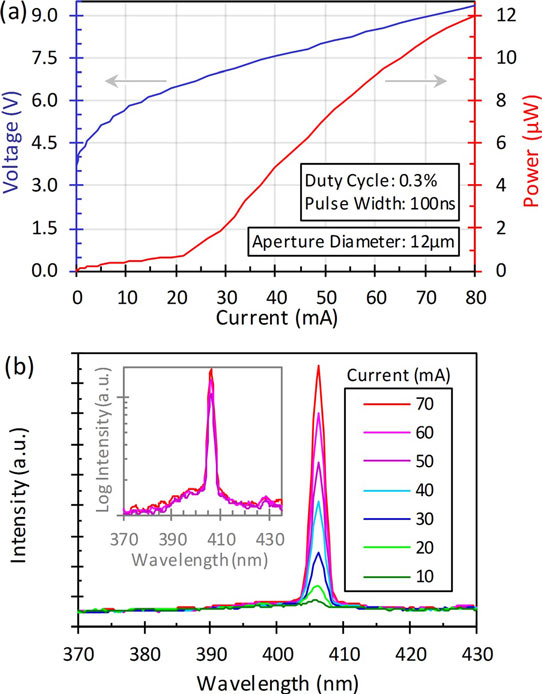
Figure 3: (a) Pulsed light output power, current, voltage (LIV) characteristics measured on 12μm-aperture-diameter VCSEL. (b) Emission spectrum versus current.
In 0.3%-duty-cycle 100ns pulse operation, the threshold current and voltage were 18mA (16kA/cm2) and 6.4V, respectively, for a 12μm-diameter aperture VCSEL. The output power was 12μW at 80mA. The emission was single-mode longitudinal at 406nm. At 70mA, the full-width half maximum (FWHM) was ~2nm. The polarization of the light was 100%.
The researchers comment: "The overall yield of these devices is markedly higher than we observed previously, though we still see a large variation in the Jth across a single chip. A number of other improvements, [. . .] include optimization of the p-DBR deposition conditions to reduce ion damage, optimization of the flip-chip bonding conditions to mitigate catastrophic increases in the operating voltage, and optimization of the Mg doping in the EBL [electron-blocking layer] to reduce Mg diffusion into the MQW."
Optical microscope inspection of the emission showed non-uniform lasing across the aperture. The non-uniformity is likely due to filamentation for which a variety of explanations have been put forward: material inhomogeneity, surface morphology, local cavity length, current spreading, lateral index fluctuations, the polycrystalline ITO contact, or poor thermal conductivity of the p-DBR. However, the researchers comment: "We believe that the filamentation (i.e. spatially non-uniform lasing) is predominately a result of non-uniform current spreading, contact resistance, absorption loss, and/or lateral index fluctuations."
http://dx.doi.org/10.1063/1.4926365
The author Mike Cooke is a freelance technology journalist who has worked in the semiconductor and advanced technology sectors since 1997.


