- News
11 February 2015
Boosting swing and transconductance in tri-gate InGaAs MOSFET
Researchers based in USA and South Korea claim a record combination of subthreshold swing (82mV/decade, 0.5V drain bias), transconductance (1800μS/μm) and on-current (0.41mA/μm) for any tri-gate quantum well indium gallium arsenide (InGaAs) metal-oxide-semiconductor field-effect-transistor (MOSFET) [Tae-Woo Kim et al, IEEE Electron Device Letters, published online 20 January 2015]. The team was based at SEMATECH Inc in the USA, KANC in South Korea, and GLOBALFOUNDRIES in the USA.
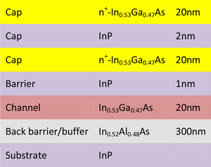
 Figure 1: Epitaxial structure for InGaAs MOSFET.
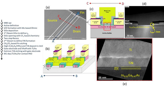
The III-V epitaxial structure was grown on semi-insulating indium phosphide (InP) by molecular beam epitaxy (MBE) – see Figure 1. A multi-layer cap was used to control the side spacing, Lside, in the combined wet/dry recess etch (Figure 2). Patterning consisted of two electron-beam lithography processes to achieve the desired fin width and gate length. The fin width and height were 30nm and 20nm, respectively.

Figure 2: Process flow, cross-sectional schematic and TEM image of a tri-gate InGaAs MOSFET, from longitudinal and horizontal direction.
The 80nm gate length was determined by an opening in a silicon dioxide (SiO2) layer. The gate insulation consisted of 0.7nm of aluminium oxide (Al2O3) and 2nm of hafnium dioxide (HfO2) deposited by atomic layer deposition (ALD).

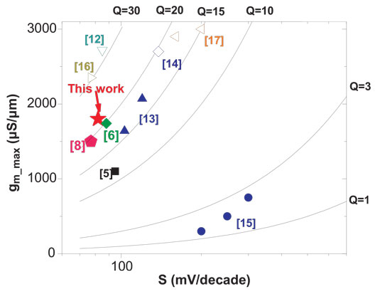
Figure 3: Maximum transconductance versus subthreshold-swing, comparing with other reports. Q is gm_max/S. Filled symbols are for III-V non-planar MOSFETs and open symbols for planar-MOSFETs. In all cases, drain bias is 0.5V.
The authors present a benchmark chart of transconductance (gm_max) versus subthreshold swing (S) to support their record claim (Figure 3).
InGaAs MOSFET InGaAs MOSFET MBE ALD
http://ieeexplore.ieee.org/xpl/abstract
The author Mike Cooke is a freelance technology journalist who has worked in the semiconductor and advanced technology sectors since 1997.


