- News
10 June 2014
UCSB reports highest-performing III-V MOSFETs
At the 2014 Symposium on VLSI Technology, University of California, Santa Barbara (UCSB) has reported what are claimed to be the highest-performing III-V metal-oxide semiconductor (MOS) field-effect transistors (FETs).
The research promises to help deliver higher semiconductor performance at lower power consumption levels for next-generation, high-performance servers. The research is supported by Semiconductor Research Corporation (SRC) of Research Triangle Park, NC, USA, the university-research consortium for semiconductors and related technologies.
The UCSB team’s III-V MOSFETs exhibit for the first time, it is reckoned, on-current, off-current and operating voltage comparable to or exceeding production silicon devices — while being constructed at small dimensions relevant to VLSI (very-large-scale integration) applications.
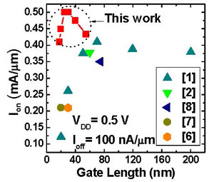
For the past decade, III-V MOSFETs have been widely studied by a large number of research groups, but none had reported a III-V MOSFET with a performance equal to, let alone surpassing, that of a silicon MOSFET of similar size. In particular, UCSB’s transistors have a gate length of 25nm, an on-current of 0.5mA and off-current of 100nA per micron of transistor width, and require only 0.5V to operate.
 Picture: Ion, at 0.5V VDS and 100nA/μm Ioff, versus Lg, compared to the III-V literature.
“The goal in developing new transistors is to reach or beat performance goals while making the transistor smaller — it is no good getting high performance in a big transistor,” says Mark Rodwell, professor of Electrical and Computer Engineering at UCSB. “In time, the UCSB III-V MOSFET should perform significantly better than silicon FinFETs of equal size,” he adds.
To reach the reported performance, the UCSB team made three key improvements to the III-V MOSFET structure.
First, the transistors use extremely thin semiconductor channels, some 2.5nm (17 atoms) thick, with the semiconductor being indium arsenide (InAs). Making such thin layers improves the on-current and reduces the off-current. These ultra-thin layers were developed by UCSB Ph.D student Cheng-Ying Huang under the guidance of professor Arthur Gossard.
Next, the transistors use very-high-quality gate insulators as dielectrics between the gate electrode and the semiconductor. These layers consist of a stack of alumina (Al2O3, on InAs) and zirconia (ZrO2), and have a very high capacitance density so that, when the transistor is turned on, a large density of electrons can be induced into the semiconductor channel. Development of these dielectric layers was led by UCSB Ph.D student Varista Chobpattana under the guidance of professor Susanne Stemmer.
Third, the transistors use a vertical spacer layer design, which distributes the field more smoothly within the transistor, avoiding band-to-band tunneling. As with the very thin InAs channel design, the vertical spacer reduces the leakage currents, allowing the transistor’s off-current to rival that of silicon MOSFETs. The overall design, construction and testing of the transistor was led by UCSB Ph.D student Sanghoon Lee under Rodwell’s guidance.
“The UCSB team’s result goes a long way toward helping the industry address more efficient computing capabilities, with higher performance but lower voltage and energy consumption,” comments Kwok Ng, senior director of Device Sciences at SRC. “This research is another critical step in helping ensure the continuation of Moore’s Law.”
Vertical spacers for tighter integration of III-V MOSFETs
www.ece.ucsb.edu/Faculty/rodwell/research_group/highfreq.html


