- News
13 June 2014
Chloride-based chemical doping yields low-contact-resistance MoS2 FETs
At the 2014 Symposia on VLSI Technology and Circuits in Honolulu, Hawaii (9-13 June), a team at Purdue University, SEMATECH of Albany, NY, USA (the international research consortium of semiconductor device, equipment, and materials manufacturers) and the State University of New York (SUNY) College of Nanoscale Science and Engineering (CNSE, where SEMATECH is based) has presented a chemical doping technique that has reduced contact resistance (Rc) by 10-fold and specific contact resistivity (ρc) by 100-fold to enable the demonstration of high-performance molybdenum disulfide (MoS2) field-effect transistors (FETs).
The paper ‘High-Performance MoS2 Field-Effect Transistors Enabled by Chloride Doping: Record Low Contact Resistance (0.5kΩ·μm) and Record High Drain Current (460μA/μm)’ was authored by Purdue doctoral students Lingming Yang, Yuchen Du, Han Liu and Heng Wu; SEMATECH researchers Kausik Majumdar, Py Hung, Robert Tieckelmann and Chris Hobbs; CNSE researcher Michael Hatzistergos; Intel’s Wilman Tsai; and Purdue professor of electrical and computer engineering Peide Ye.
The research is said to be an important milestone for the realization of ultra-scaled low-power two-dimensional (2D) MoS2 FETs and the advancement of photonic and electronic devices based on transition metal dichalcogenide (TMD) materials such as solar cells, photo-transistors and low-power logic FETs. The work is supported by SEMATECH and Semiconductor Research Corporation (SRC) of Research Triangle Park, NC, USA (the university-research consortium for semiconductors and related technologies).
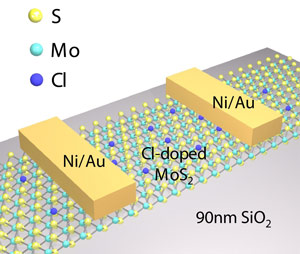
As part of the research, the team leveraged MoS2, which has been studied closely by the semiconductor industry in recent years due to its potential applications in electrical and optical devices. However, high contact resistance significantly limits the device performance of MoS2 FETs. One method for resolving this is to dope the MoS2 film, but doping the atomically thin film is non-trivial and requires a simple and reliable process technique. The technique used by the research team provides an effective and straightforward way for ‘molecular layer doping’ of the MoS2 film with the chloride-based chemical doping reagent 1,2 dichloroethane (DCE) to significantly reduce the contact resistance.
 The structure of extremely thin MoS2 (a single-atomic layer of molybdenum sandwiched between single-atomic layers of sulfide and doped with DCE), which is particularly promising for future thin, flexible and transparent electronic devices for displays, touch pads and other applications. (Purdue University photo/Lingming Yang)
“Compared with other chemical doping materials such as PEI (polyethylene imine) and potassium, our doping technology shows superior transistor performance, including higher drive current, higher on/off current ratio and lower contact resistance,” says Ye.
To obtain high-performance FETs, three parts of the device need to be carefully engineered: the semiconductor channel (carrier density and its mobility); the semiconductor-oxide interface; and the semiconductor-metal contact. The research is particularly aimed at eliminating the last major roadblock toward demonstration of high-performance MoS2 FETs, namely high contact resistance.
Fabricated at Purdue, the MoS2 FETs using the doping technique can now be reproduced in a semiconductor manufacturing environment and show the best electrical performance among all the reported TMD-based FETs, it is claimed. The contact resistance (0.5kΩ·μm) with the doping technique is 10 times lower than the controlled samples. The drive current (460μA/μm) is twice that of the best value in prior literature.
“Due to recent advances such as the research being presented at the VLSI Symposium, 2D materials are gaining a lot of attention in the semiconductor industry,” says Satyavolu Papa Rao, SEMATECH’s director of Process Technology. “The collaborative effort among world-class researchers and engineers from this team is a prime example of how consortium-university-industry partnerships further enable the development of cutting-edge process techniques,” he adds.
“Improved contacts are always desirable for all electronic and optical devices,” notes Kwok Ng, senior director of Device Sciences at SRC. “The doping technique presented by this research team provides a valid way to achieve low contact resistance for MoS2 as well as other TMD materials.”
www.sematech.org/research/materials
https://engineering.purdue.edu/~yep


