- News
9 July 2014
Gallium nitride thin-film transistors produced at less than 250°C
Turkey’s Bilkent University has used hollow-cathode plasma-assisted atomic layer deposition (HCPA-ALD) to make gallium nitride (GaN) thin-film transistors (TFTs) at temperatures below 250°C [S. Bolat et al, Appl. Phys. Lett., vol104, p243505, 2014]. The researchers claim this as the lowest reported process temperature for GaN transistors.
Thin-film transistors are usually produced using amorphous silicon. While these devices are used as the driving element in liquid crystal displays, low carrier mobility, high fabrication thermal budget, and strong absorption of visible light limits applications and is not suitable for flexible and transparent electronics.
Zinc oxide and related materials have recently been developed as an alternative, with characteristics matching or even bettering silicon-based devices. However, ZnO TFTs suffer from stability issues.
GaN could be a stable base material, but the compound is usually processed at temperatures exceeding 1000°C. Such temperatures would generally destroy the other components for which the TFTs are the driving element.
Bilkent’s very low process temperature results in polycrystalline material. Although the performance for these first simple bottom-gate devices was not particularly impressive, the researchers see potential for the GaN-based devices as stable flexible/transparent TFT devices after further materials and process optimization.
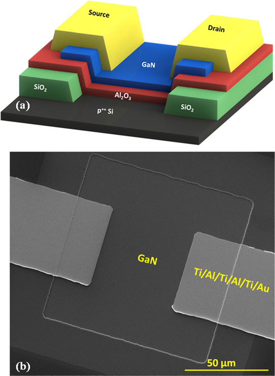
The Ga precursor for the HCPA-ALD was trimethyl-gallium. The nitrogen was supplied as N2 in a hydrogen carrier. The plasma power was 300W and the temperature was 200°C. The TFT structure (Figure 1) was defined using a 200nm 250°C plasma-enhanced chemical vapor deposition (PECVD) silicon dioxide mask.

Figure 1: (a) 3D schematic of the HCPA-ALD-based GaN TFT; (b) SEM image of the fabricated device.
Layers of 77nm aluminium oxide and 11nm GaN were deposited in a window in the SiO2 at 200°C using a modified Fiji 200-LL ALD reactor from Ultratech/Cambridge NanoTech Inc. X-ray analysis showed the GaN film to be polycrystalline with average crystallite size of 9.3nm. The aluminium oxide provided the gate insulator and the GaN provided the channel; the bottom gate was the p++-silicon substrate itself.
The active region was isolated using an argon-based plasma etch. The source-drain electrodes consisted of titanium/aluminium/titanium/aluminium/titanium/gold. The metal stacks were not annealed to keep the thermal budget as low as possible. The length and width of the resulting device were both 50μm.
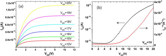
The devices had an on/off ratio of 2x10³ with a drain bias of 1V (Figure 2). Gate leakage was less than 0.5pA for all bias conditions. The threshold voltage was 11.8V, giving an n-type enhancement-mode (normally off) operation. The subthreshold swing was 3.3V/decade. The effective charge mobility was 0.025cm2/V-s. The researchers comment: “This particularly low mobility can be attributed to the nanocrystalline structure of the HCPA-ALD based GaN thin films, and the surface states at the semiconductor insulator interface.”

Figure 2: (a) Output and (b) transfer characteristics of HCPA-ALD-based GaN TFTs.
Positive bias stress testing was carried out with measurement of the threshold voltage after applying a field of 2.5MV/cm between the gate and grounded source-drain electrodes. A shift in threshold voltage indicates charge trap states at semiconductor/insulator interfaces or within the aluminium oxide. The shift increased with duration of the stress stage of the test. At 200 seconds, the shift was around 5.5V; this increased to 7.3V for 1000 seconds of stressing. The researchers point out that the 1000-second shift in high-performance zinc oxide-based TFT is larger.
HCPA-ALD GaN Thin-film transistors
http://scitation.aip.org/content/aip/journal/apl/104/24/10.1063/1.4884061
The author Mike Cooke is a freelance technology journalist who has worked in the semiconductor and advanced technology sectors since 1997.


