- News
3 December 2014
Boron nitride releases GaN transistors from self-heating degradation
NTT Basic Research Laboratories in Japan has used a hexagonal boron nitride (h-BN) layer to release and transfer gallium nitride (GaN) high-electron-mobility transistors (HEMTs) from sapphire substrate to thermally conducting copper, improving performance [Masanobu Hiroki et al, Appl. Phys. Lett., vol105, p193509, 2014]. The same team has previously used h-BN to grow and transfer GaN-based LEDs in a similar manner [Mechanical release of nitride semiconductors from sapphire using a boron nitride layer].
The researchers used c-plane sapphire as the growth substrate. Although GaN growth on sapphire is well established, self-heating effects in the operation of the resulting devices can cause degradation of performance. Sapphire has a low thermal conductivity of 40W/mK, compared with 150W/mK for silicon, 350W/mK for silicon carbide, or 600-2000W/mK for diamond. However, these alternatives either suffer from a poor lattice match with GaN or are extremely expensive.
The h-BN layer was grown using triethylboron and ammonia (NH3) as precursors for metal-organic vapour phase epitaxy. Hexagonal BN has a similar crystal structure to graphite, allowing easy cleavage. The further device layers consisted of 100nm aluminium nitride (AlN) nucleation, 3μm GaN buffer, and 32nm Al0.27Ga0.73N barrier.
The transistor fabrication included mesa etch for electrical isolation, and ohmic contact and Schottky gate formation. The titanium/aluminium/nickel/gold ohmic contacts were annealed. The gate metals were nickel/gold. The gate was 1.5μm long and 100μm wide. The source-drain spacing was 6μm.

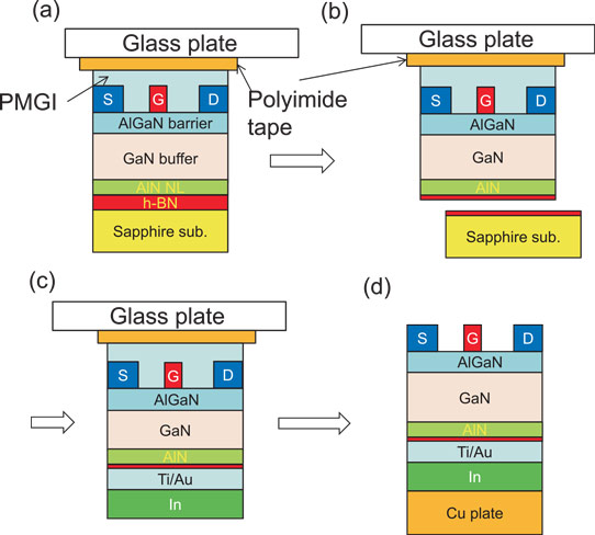
Figure 1: Schematic process sequence for transfer of AlGaN/GaN HEMT from sapphire substrate to copper plate. (a) Temporary adhesion of HEMT to glass plate with polyimide tape. (b) Mechanical release of HEMT from sapphire by cleavage of h-BN layer. (c) Ti/Au and In deposition on backside of sample. (d) Adhesion of sample to copper plate by thermal bonding and release from glass.
The transfer process consisted of coating the sample with polymethylglutarimide (PMGI) and attaching it to glass with polyimide tape (Figure 1a). The sapphire substrate was then mechanically removed, cleaving the h-BN release layer (Figure 1b). The titanium/gold was deposited on the backside of the sample, followed by electroplating 1μm of indium (Figure 1c). Thermal fusion bonding at 180°C was then used to attach the devices to thermally conductive copper (Figure 1d). The bonding temperature was above the melting point of indium. The thermal conductivity of the copper was 390W/mK. The glass was removed by dissolving the PMGI in organic solvent.
Growing nitride semiconductor materials on h-BN was found to increase dislocation densities by about an order of magnitude, according to x-ray analysis. However, the increase in dislocation density was not found to impact the Hall mobility of 1360cm2/V-s or sheet electron density of 7.4x10¹²/cm2. The researchers point out that dislocations are not believed to be the dominant electron scattering mechanism at the dislocation density estimated.

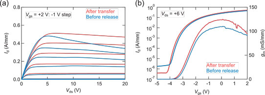
Figure 2: Drain current-voltage (Id-Vds) characteristics of AlGaN/GaN HEMTs before release from sapphire (blue line) and after transfer to a copper plate (red line). (b) Drain current- and transconductance-gate voltage (Id-Vgs, gm-Vgs) transfer characteristics at 6V drain bias.
The transfer to copper plate improved the drain current flow at high drain bias (Figure 2). Before transfer to copper, the drain current peaks - giving ‘saturation’ - and then falls off significantly (negative differential resistance). With a 2V gate potential, the fall from saturation to 20V drain bias was 30%. In a device on copper, the fall was only 8%. The negative differential resistance effect is typically attributed to self-heating.
Another benefit of transfer to copper was an increased transconductance: 120mS/mm with 6V drain bias, compared with 100mS/mm before transfer. The threshold voltage of the devices was -3.5V, both before and after transfer.
Infrared images suggested that the peak temperature of transistors at 20V drain bias was 50°C before and 30°C after transfer to copper. The drain currents were 40mA and 50mA, respectively. The corresponding power dissipations were 0.8W and 1W.
Boron nitride GaN HEMTs GaN HEMTs Sapphire substrates
http://dx.doi.org/10.1063/1.4901938
The author Mike Cooke is a freelance technology journalist who has worked in the semiconductor and advanced technology sectors since 1997.


