- News
22 April 2014
EVG leading in permanent bonding market, but merged Applied/Tokyo Electron to challenge
With silicon-on-insulator (SOI) business declining, 3D TSV stack implementation beginning, and the competitive environment changing, market research firm Yole Développement has released a new study ‘Permanent Wafer Bonding for Semiconductor: Application Trends & Technology Report’.
The permanent bonding equipment market is currently dominated and fragmented by three main suppliers - EV Group (EVG), SUSS MicroTec, and Tokyo Electron (TEL) - accounting for almost 80% of the market by focusing on micro-electro-mechanical systems (MEMS) and advanced packaging applications including backside-illuminated (BSI) CMOS image sensors (CIS), CIS capping wafer-level packaging (WLP) and 3D stack through-silicon vias (TSV).

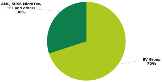
Picture: 2013 market share breakdown by permanent bonding equipment supplier (in $m).
EVG is still the market leader, with more than 70% share, but will be challenged by the merging of TEL and Applied Materials (AMAT), two of the world’s largest semiconductor equipment suppliers, says Yole. In particular, TEL has gained permanent bonding market share in 2013, especially due to its deep involvement in 3D TSV stack bonding technology performed at room temperature.
Other big equipment suppliers have created a challenging environment and stimulated technology innovation for further improvements in the advanced packaging area.
Also, the entrance of aggressive new players is likely to challenge established players. Some players such as Mitsubishi Heavy Industry (MHI) have recently entered the market via low barriers of entry, mainly with customers involved in the R&D sector;
However, the merger of TEL and AMAT brings into question the involvement of permanent bonding equipment suppliers in future, says Yole.
In parallel, SUSS MicroTec, which has provided automated bonders for production applications for 10 years, has ceased making them in 2013, demonstrating that the permanent bonding market is very challenging.
TSV integration creating growth in permanent wafer bonding
Permanent bonding technology is a key process for a wide range of semiconductor applications such as MEMS, advanced packaging (BSI CIS, CIS capping WLP, 3D stack TSV), LED devices, and silicon-on-insulator (SOI) substrate applications. This type of application is quite complex due to the high diversity of existing bonding technologies.

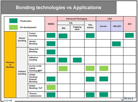
Picture: Bonding technologies versus applications.
Permanent bonding is currently being applied in:
- a large quantity of MEMS devices supported by glass frit and anodic bonding technologies in order to achieve good hermeticity to protect the MEMS sensor;
- LEDs requiring metal bonding (eutectic and thermo-compression bonding) in order to achieve higher performance in terms of light extraction;
- CMOS image sensors: BSI CMOS image sensor where one bonding step is required at the front-end, and CIS capping WLP to bond the glass cap wafer to the device; and
- SOI substrate manufacturing supporting the fusion bonding technology.
These have been the four main applications for permanent bonding for several years, and permanent bonding processes are becoming increasingly important within the semiconductor industry.
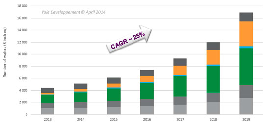
The total permanent bonding market generated almost 5 million 8”-equivalent bonded wafers, driven mostly by the established applications - BSI CIS and MEMS devices - and is expected to peak at more than 16 million 8”-equivalent bonded wafers in 2019. Demand for permanent bonding is growing, driven mainly by the miniaturization required for 3D stack TSV applications.
Cu-Cu bonding at room temperature could change the game
The total permanent bonding market generated revenue of about $65m in 2013, relying mostly on anodic bonding, fusion bonding and glass-frit bonding technologies. It is expected that this will rise at a compound annual growth rate (CAGR) of 25% to almost $250m in 2019, fueled by the Cu-Cu bonding/oxide hybrid technique performed at room temperature.

Picture: Wafer_Forecast by application (in 8-inch equivalents): 3D TSV stack, BSI CIS, CIS capping WLP, LED carrier, LED packaging, MEMS, SOI.
New technical developments along the way will be needed for the next generation of MEMS, LED and advanced packaging applications. In the next few years, the permanent bonding market will be supported by metal bonding and bonding performed at room temperature.
Indeed, it seems that the most promising permanent bonding technology for future applications based on 3D interconnects is certainly metal bonding or Cu-Cu/oxide hybrid bonding performed at room temperature. Every major player is now working on the implementation and qualification of this technology for the new generation of BSI CIS arrays and for 3D stack TSV. However, there are still several challenges associated with this emerging permanent bonding process integration related to its reliability at room temperature. Some work remains to be done to achieve good enough performance for production, says Yole.
Specifically, in the 3D stack TSV market, electrical and mechanical properties will be the key to competing with other permanent bonding technologies.


