- News
27 September 2013
Copper with titanium nitride offers alternative GaN HEMT gate stack
Taiwan’s National Chiao-Tung University has developed a titanium nitride/copper (TiN/Cu) gate structure for aluminium gallium nitride (AlGaN) high-electron-mobility transistors (HEMTs) that shows improvements over a comparison nickel/gold stack [Yueh-Chin Lin et al, Appl. Phys. Express, vol6, p091003, 2013].
Among the motivations for the switch in gate materials, the researchers cite recent price increases in gold. Attractions for a copper-based gate include good electrical conductivity, high melting point, high thermal stability, good adhesion to dielectrics, and lower cost.
However, copper cannot be simply applied since the metal would diffuse quickly into the AlGaN barrier, reducing the Schottky barrier and degrading transistor performance. Thus, a thin layer of TiN is needed as a barrier against copper diffusion into the AlGaN.
The titanium nitride/copper (TiN/Cu) gate electrodes were applied to epitaxial material consisting of GaN buffer and AlGaN barrier. The HEMT fabrication consisted of mesa isolation, and ohmic contact and gate formation. The ohmic contacts comprised an annealed stack of titanium/aluminium/nickel/gold metals. The annealing was carried out at 800°C for a minute in nitrogen.
The TiN/Cu (50nm/200nm) gate was applied using reactive sputtering. The TiN source was a titanium metal target in nitrogen/argon atmosphere under 200V DC power. The gate length was 2μm. A comparison device with a nickel/gold (50nm/200nm) gate was also produced on the same epitaxial wafer.
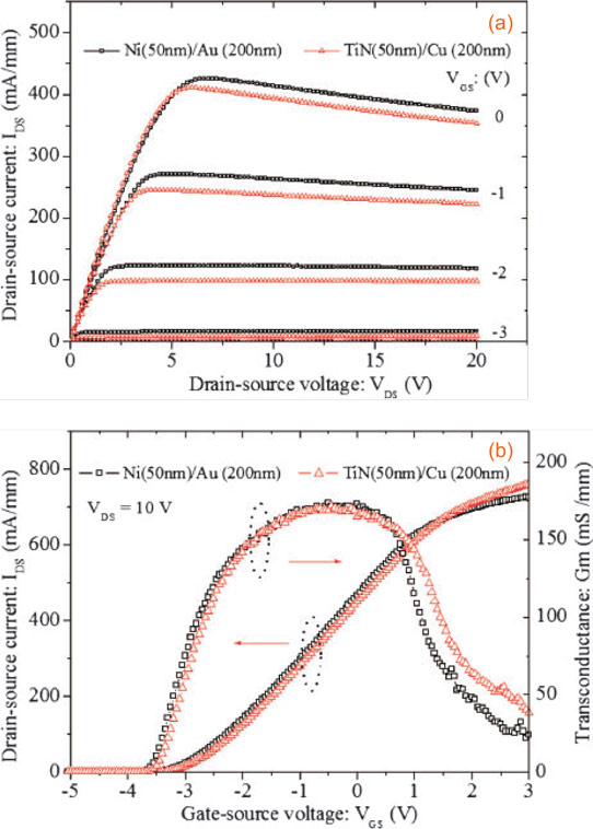
The DC characteristics of the TiN/Cu gate structure showed higher maximum drain current at 3V gate potential than the Ni/Au electrode (Figure 1). The researchers attribute this to the higher Schottky barrier height of TiN on GaN. Also, the OFF-state breakdown voltage was edged up from 325V for the Ni/Au device to 346V for the TiN/Cu HEMT.

Figure 1: Comparison of DC characteristics for TiN (50nm)/Cu (200nm)- and Ni (50nm)/Au (200nm)-gated AlGaN/GaN HEMTs: (a) drain current (IDS) versus voltage (VDS) curves, and (b) transconductance (Gm) and drain current (IDS) versus gate potential (VGS) curves.
High-voltage stress tests were carried out on both devices for up to 3 hours with 200V drain and -5V gate potentials. The source-drain and gate-drain distances were 20μm and 15μm, respectively. Both device types showed current degradation that could be attributed to electrically induced mechanical stress creating defects in the AlGaN barrier and/or near the gate edge. Also playing a role is charge injection from the gate electrode.
For 1 hour stress, the drain current was reduced to 70% (down 30%) of the unstressed value in the Ni/Au HEMT, compared with the 93% result for the TiN/Cu gate (down 7%). The researchers comment: “The smaller current degradation for the TiN/Cu-gated HEMT indicates that TiN is more stable than Ni on AlGaN, and fewer electrical defects were produced for the TiN/Cu-gated HEMTs than for the Ni/Au-gated HEMTs. This may be caused by the fact that it is easier for Ni to react with AlGaN when the device was under high-voltage stress.”
The longer 3 hour stress resulted in degradation of the drain current of 35% and 19% for the Ni/Au and TiN/Cu gates, respectively. Some 10 minutes after the stress, the degradations had recovered, respectively, to 17% and 4%. This indicates that much of the injected charge was released.
The researchers also performed extended 200V high-voltage stress testing up to 32 hours for OFF-state drain and gate currents, along with ON-state drain current. The ON drain current reduced from 400mA/mm to 372mA/mm over the period for the TiN/Cu HEMT. The OFF drain and gate currents remained around 0.4mA/mm and 0.3mA/mm over the period. The Ni/Au HEMT showed rapid degradation in ON drain current, failing after 10 hours.

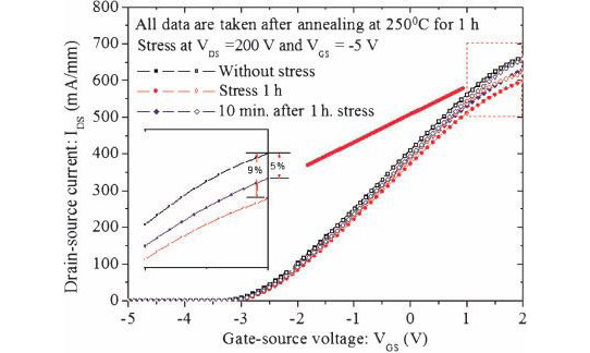
Figure 2: IDS versus VGS curves for TiN (50nm)/Cu (200nm)-gated AlGaN/GaN HEMTs annealed at 250°C for 1 hour for device without high-voltage stress, with high-voltage stress and 10 min after the high-voltage stress was terminated.
Thermal stability testing consisted of annealing at 250°C for 1 hour. The TiN/Cu device showed no change in performance. After an hour of high-voltage stress the drain current was down 9% (Figure 2). The performance was restored after 10 minutes, indicating that “the TiN/Cu gate structure has excellent thermal stability”. The Ni/Au HEMT subjected to thermal and a few minutes of high-voltage stress failed after a few minutes.
http://apex.jsap.jp/link?APEX/6/091003
The author Mike Cooke is a freelance technology journalist who has worked in the semiconductor and advanced technology sectors since 1997.


