- News
29 October 2013
Palladium oxide interlayer cuts gate leakage in nitride HEMTs
Researchers in Taiwan have used a palladium oxide (PdO) gate interlayer to improve nitride semiconductor high-electron-mobility transistor (HEMT) performance [Ray-Ming Lin et al, Jpn. J. Appl. Phys., vol52, p111002, 2013]. In particular, the on/off current ratio was increased by three orders of magnitude and the subthreshold swing was halved over devices using pure palladium in the gate. The researchers were based at Chang Gung University and National Taiwan University.
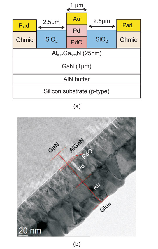
The HEMT structures (Figure 1) were grown on high-resistivity p-silicon wafers of 6-inch diameter using metal-organic chemical vapor deposition (MOCVD). The devices were isolated by etching down to the GaN buffer to create a mesa. The ohmic source-drain contacts were thermally annealed titanium/aluminium/nickel/gold.

Figure 1: (a) Schematic cross-sectional image of GaN/AlGaN/PdO/Pd–Au HEMTs. (b) TEM image of GaN/AlGaN/PdO/Pd–Au structure.
The gate stack was formed by patterning, evaporation of palladium in oxygen to create a 10nm PdO layer, and then deposition of more palladium (70nm) and 140nm of gold. Devices without the PdO layer were also produced.
Further processing for device interconnection and probe pads and passivation consisted of titanium/gold evaporation and silicon dioxide deposition.
Averaged over ten randomly selected devices, the maximum drain current at 2V gate potential was 430mA/mm for the HEMT with a PdO layer in the gate stack and 402mA/mm without. The slightly higher drain current with PdO layer is attributed to a passivating effect increasing the carrier density in the two-dimensional electron gas (2DEG) near the AlGaN/GaN interface that acts as the conductive channel between the source and drain.
The researchers believe that the improved on-resistance can be attributed to the higher work function of up to 7.9eV for PdO. The high work function also creates a higher Schottky barrier of 0.884eV between the gate stack and AlGaN barrier layer, compared with 0.716eV for the HEMT without PdO.
Pinch-off occured at -3.6V for both types of HEMT. The PdO layer improved the on/off current ratio and subthreshold swing. The on/off ratio at 8V source-drain bias was increased by three orders of magnitude from 9.5x10⁵ for the device without PdO to 1.2x10⁹ with PdO. The off current leakage was 7.1x10⁻⁴mA/mm for the device without PdO and 4.3x10⁻⁸mA/mm with PdO.
The subthreshold swing was halved to 66mV/decade from 122mV/decade. Both of these features suggest “excellent gate control of the 2DEG channel” with a PdO layer in the gate stack. Using the subthreshold swing, the researchers estimate that the effective trap state density in the PdO-HEMT was reduced to 2.04x10¹¹/eV-cm2 from 2.08x10¹²/eV-cm2 in the device without PdO.

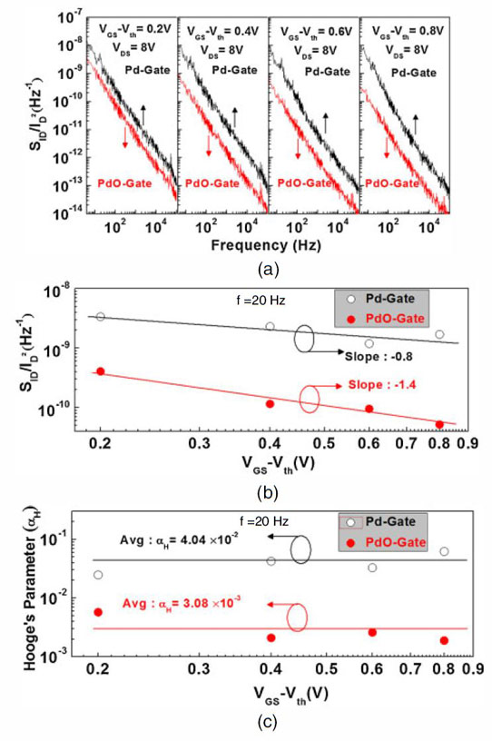
Figure 2: (a) Normalized current spectral density (SID/ID2) with various gate overdrive (VGS – Vth) values; (b) SID/ID2 versus VGS – Vth at fixed frequency of 20Hz; (c) Hooge’s coefficient versus VGS – Vth for both PdO- and Pd-Gate HEMTs.
Low-frequency noise measurements (Figure 2) were carried out with the help of Taiwan’s National Nano Device Labs (NDL). The low gate leakage of the PdO gate stack also reduced flicker (1/f) noise in the low-frequency range 1Hz-100kHz. The Hooge coefficient that normalizes flicker noise current spectral density, taking account of device structure and material, was 4.04x10⁻² without PdO in the gate stack. This was reduced to 3.08x10⁻³ with the PdO layer. The researchers also expect the introduction of PdO to reduce shot noise that affects high-frequency performance.
http://jjap.jsap.jp/link?JJAP/52/111002
The author Mike Cooke is a freelance technology journalist who has worked in the semiconductor and advanced technology sectors since 1997.


