- News
14 November 2013
Diamond materials for semiconductors to grow to $43m market in 2020, driven by passive devices
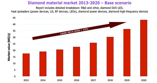
Driven mainly by heat spreaders for high-power device thermal management, the diamond materials market for semiconductor devices will rise at a compound annual growth rate (CAGR) of 14% to more than $43m in 2020, according to the base scenario in a new report ‘Diamond materials for semiconductor applications’ from market research firm Yole Développement that considers both passive (heat spreaders) and active (diodes, transistors) diamond solutions.

Diamond materials have been in development for more than 50 years. Besides the traditional tooling applications (drilling, cutting etc), interest in diamond continues to grow for optical and thermal applications, and for new applications in semiconductor devices such as high-power devices and high-frequency devices able to work at elevated temperatures.
In fact, diamond’s unique physical and electrical properties - which include the highest known thermal conductivity, a wide bandgap energy, excellent electrical insulator properties, very high breakdown voltage, and very high carrier mobility - make diamond an excellent candidate for electronic devices with ultimate performance.
Applications in electronic devices include high-voltage power electronics, high-frequency high-power devices, and high-power optoelectronic devices (laser diodes, LEDs). Despite the high costs of high-quality materials, a large number of players are involved in the 2013 diamond materials market and its largest segment (R&D activities), reckons Yole.
However, the costs of diamond - as well as the remaining technology barriers - limit the diamond material market to just a few applications and some high-end devices.
Access to high-quality diamond material is key for device development
Electronic applications (such as Schottky diodes, transistors etc) require high-quality single-crystalline diamond grown by chemical vapour deposition (CVD), which has superior characteristics such as high carrier mobility, long carrier lifetimes, high breakdown fields and high thermal conductivity.
High-quality low-defect diamond wafers produced from diamond crystal made by the high-pressure high-temperature (HPHT) method are only a few millimeters in size. In comparison, the competing semiconductor materials such as silicon carbide (SiC) are already available in wafer sizes up to 150mmin diameter. For future diamond-based active devices, it is crucial to increase wafer size above 2-inch, with defect density of 100cm-2 or less. Different approaches to obtaining free-standing wafers from thick diamond films are under development. A mosaic-type method is currently approaching 2-inch wafer size, but the defect density needs to be reduced. According to Yole’s technology roadmap for single-crystal diamond wafers, low-defect 2-inch wafers could be commercially available in 2016-2017.
Alternatively, the microwave-enhanced chemical vapor deposition (MWCVD) approach for crystal growth is more promising than HPHT, due to its potential for scaling. MWCVD is also the most promising technique for thin-film growth, details the report. High-quality thick diamond films can be grown by homoepitaxy on single-crystal diamond wafers.
The heteroepitaxy of diamond on iridium enables diamond films of up to 4-inch in size, but further development is needed to obtain a well-controlled and reproducible manufacturing process.
Apart from the technology challenges related to single-wafer material manufacturing, electronic applications of diamond are severely hampered by the fact that n-type doping is still relatively difficult to obtain due to the lack of an efficient charge donor. As p-type doping of normally insulating diamond can now be reliably achieved using boron, much activity has been focused on the fabrication of unipolar devices. The first expected active diamond power devices will be Schottky diodes.
Although polycrystalline films have inferior electric and thermal properties compared with single crystal material, they are available in larger dimensions and at lower costs. As shown in the report, they are used mainly as heat spreaders (plus many non-electronic applications, such as optical windows, etc).

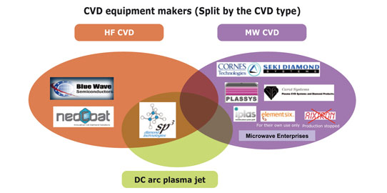
Future cost reduction and performance improvement of diamond films relies strongly on the CVD equipment that is used. Much effort from equipment makers such as Cornes Technologies (Seki Diamond), Element Six, Plassys-Bestek, sp3 Diamond Technologies etc is hence being focused on the development of CVD reactors with a larger deposition area, higher growth rate, lower electricity consumption and better film quality. The ‘integration’ of diamond film directly into a wafer (used for the fabrication of electronic and opto devices, as done for instance in Group4 Labs’ GaN-on-diamond approach) has great potential to reduce the cost of heat management solutions for high-power and high-frequency applications, says Yole.
Earlier market entry to secure better position in future market
Differentiation between diamond material suppliers is mainly through technology. Although many players are currently able to supply diamond material, only a few can supply high-quality material, providing greater differentiation compared to lower-performance but less costly non-diamond alternatives. In fact, fewer than three companies per material type can consistently deliver high-quality products. Many players have significant R&D activity underway to develop new products and access dedicated R&D funding, as well as to maintain any technological advantages that they have over the competition.
The recent acquisition of Group4 Labs by Element Six (a member of De Beers Group) indicates the trend to maintain key technologies within a select group of players, providing them with a well-established position in the diamond material market. History tells is that the development and optimization of diamond technologies is complex and takes many years. During this period, the historical diamond players will acquire a significant technological and IP advantage, which may be hard for new players to overcome and makes it nearly impossible to enter the market in the future, reckons Yole.
The developers/manufacturers of high-performance devices (such as high-power and high-frequency devices and high-power optoelectronics) rely on the reproducible supply of high-quality materials. Leading European and Japanese companies - especially those involved in the power electronic business - are still quite conservative with regard to using diamond-based devices. This provides an opportunity for other companies to take a lead in this market segment and to progressively develop their market share in power electronics by avoiding the direct competition within the established technologies, concludes Yole.
Element Six acquires Group4 Labs to expand portfolio of synthetic diamond materials
DARPA awards TriQuint contract to triple performance of GaN-based RF PAs
www.i-micronews.com/upload/Rapports/


