- News
27 June 2013
Nitride semiconductor on graphene promises 1THz performance
The US Naval Research Laboratory (NRL) in Washington DC has developed a method to grow epitaxial nitride semiconductors on graphene [Neeraj Nepal et al, Appl. Phys. Express, vol6, p061003, 2013]. The researchers hope that this could lead to high-speed current-switching applications using devices such as hot-electron transistors (HETs).
Present HETs use heavily doped semiconductor or metal base regions. Heavy doping hampers ballistic transport due to impurity and carrier-carrier scattering effects. Metal base regions suffer from electron reflection effects at the base-collector interface. The NRL team believes that using graphene as the base region, in conjunction with nitride semiconductors, could lead to devices with cut-off frequencies greater than 1THz (1000GHz).
Up to now, growth of nitride semiconductors on graphene has resulted in non-uniform GaN crystallites and not a continuous film.
The NRL method includes a functionalization step that produces “for the first time” nitride semiconductor layers of a quality similar to that obtained by traditional growth methods on conventional sapphire substrates. In fact, the crystal quality is achieved with thinner layers of less than 1μm compared with layers on other substrates.
The researchers comment: “These results support a successful demonstration of electronic-quality, heteroepitxial wurtzitic GaN on graphene that is currently unavailable and can improve the performance of present state-of-the-art devices such as HETs.”
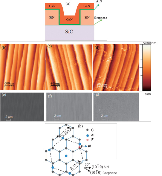
The initial epitaxial graphene (EG) layer was prepared on 4° 4H-polytype silicon carbide (1.6mm x 1.6mm squares) using silicon sublimation. Silicon nitride was then applied using plasma-enhanced chemical vapor deposition (PECVD). The silicon nitride was patterned into discs of various diameters between 50μm and 500μm.
The exposed graphene was ‘functionalized’ by subjecting it to six 30 second pulses of xenon difluoride (XeF2) plasma. The functionalization consists of creating fluorine-carbon bonds at 6-7% of sites. The bonds are semi-ionic and have been found to preserve the structural and electrical integrity of the graphene and at the same time provide nucleation sites for high-quality material deposition.
The nitride semiconductor deposition process must initially ensure that the fluorine atoms are not dislodged, so a low-temperature nucleation is needed. Unfortunately, standard techniques such as molecular beam epitaxy (MBE) and metal-organic chemical vapor deposition (MOCVD) require temperatures of more than 500°C up to around 1300°C.
The NRL nitride semiconductor deposition began instead with 280°C atomic layer epitaxy (ALE) of 11nm of aluminium nitride (AlN) as a nucleation layer. The lattice mismatch between graphene and AlN is 4.5%, compared with the 13% difference between AlN and sapphire.
The ALE was performed using a ‘Fiji’ reactor from Cambridge NanoTech. The first five pulses of precursor were of pure trimethyl-aluminium (TMA), designed to promote reaction with the fluorine atoms.
The researchers suggest that the reaction of TMA molecules with the surface fluorine atoms results in a substitution of aluminium for fluorine and the creation of reaction sites for subsequent AlN growth.
Further growth consisted of TMA and nitrogen gas pulses in argon carrier. Unreacted chemicals were purged between pulses with argon. The 11nm AlN layer was grown using 150 cycles. The thickness was determined from an AlN layer grown in the same chamber on a (111) silicon ‘witness’ substrate. Further growth of 800nm gallium nitride (GaN) semiconductor was performed using metal-organic chemical vapor deposition in a CVD Inc system.

Figure 1: (a) Schematic of GaN/AlN/graphene/SiC layered structure, (b) atomic force microscope (AFM) image as-synthesized epitaxial graphene, (c) AFM image 1.2nm ALE AlN/graphene, (d) AFM image GaN/graphene, (e) scanning electron microscope (SEM) image pristine graphene, (f ) SEM image 1.2nm ALE AlN/graphene, (g) SEM image GaN on AlE AlN/graphene. (h) Al atoms replace F atoms, creating an AlN nucleation site on graphene resulting in proposed crystalline alignments.
The material structure (Figure 1) was subjected to a large range of measurements and characterizations during processing. Raman spectroscopy was used to confirm that the growth preserved the graphene underlayer.
X-ray diffraction studies showed the GaN to have a wurtzite with rocking curve full width at half maximum (FWHM) values of 544arcsec and 461 arcsec for the (0002) and (0004) peaks, respectively. These values are similar to those obtained with 5μm GaN on sapphire with a 16% lattice mismatch.
“The similarity of these FWHMs for an order of magnitude thinner GaN film may indicate that a better crystalline quality material on EG can be achieved,” the researchers comment.
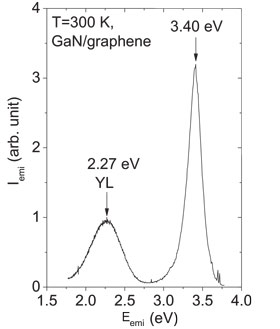
 Figure : Room-temperature photoluminescence spectra of GaN on AlN/graphene/SiC stack. Near-band-edge emission at 3.40eV, broad yellow line at 2.27eV due to presence of Ga vacancy and oxygen complex point defect.
Photoluminescence (PL) spectra show a 3.40eV band edge and a broad yellow line at 2.27eV (Figure 2). The band-edge emission could be due to either exciton (electron-hole bound pair) or direct interband recombination. The researchers believe that the yellow line is due to a Ga-vacancy/oxygen complex point defect.
The researchers conclude: “The heteroepitaxial growth of GaN on ALE AlN/EG resulted in a less strained, high-crystalline-quality GaN material under optimized growth conditions. Hence, the optimum properties of both GaN and graphene can be utilized for device applications such as HETs.”
HETs GaN-on-graphene GaN Graphene
http://apex.jsap.jp/link?APEX/6/061003
The author Mike Cooke is a freelance technology journalist who has worked in the semiconductor and advanced technology sectors since 1997.


