- News
14 January 2013
Air-channels and nanoporous structure boost output from nitride LEDs
Taiwan’s National Chung Hsing University has used nitride semiconductor growth on gallium nitride nanocolumns and nanoporosity achieved with photoelectrochemical etching to boost the light output power of light-emitting diodes (LEDs) by up to 1.75x [Ren-Hao Jiang et al, Appl. Phys. Express, vol6, p012103, 2013].
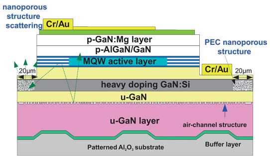
The researchers used metal-organic chemical vapor deposition (MOCVD) on patterned sapphire to grow the epitaxial material for the LEDs (Figure 1). The first two layers consisted of 30nm of low-temperature GaN (550°C) as a buffer, followed by 6μm of high-temperature undoped (u-)GaN (1150°C) as template.

Figure 1: Schematic structure of LED with nanoporous and air-channel regions (NA-LED).
The nanorod layer was formed using a 75Å-thick layer of nickel that was self-assembled into clusters by a rapid thermal anneal at 850°C in nitrogen for 90 seconds. The exposed GaN surface was reactive-ion etched. The nickel was removed by nitric acid solution, leaving nanorods that were 200-400nm in diameter and 0.5μm high.
The MOCVD process was then continued with 2μm of u-GaN (1150°C), 2μm of heavily doped n-GaN, 0.5μm of lightly doped n-GaN, a nine-period multi-quantum well layer (In0.2Ga0.8N/In0.01Ga0.99N, 3/13nm, 830°C), a six-period electron-blocking layer (Al0.3Ga0.7N/GaN, 2/2nm, 950°C), and, finally, 0.13μm of p-GaN.
The photoelectrochemical (PEC) process was preceded by cleaving the 2-inch wafer into two halves, and isolation using a triple-frequency ultraviolet Nd:yttrium aluminium garnet (355 nm) laser. The PEC etch process was performed with 0.5M oxalic acid, 0.5V DC bias, and illumination by a 400W mercury lamp. The PEC etch mainly attacked the heavily doped n-GaN layer, giving a nanoporous structure of ~0.1μm-diameter triangular holes. This region extended laterally about 20μm into the n-GaN layer from the laser scribe line. The PEC etch also reduced the diameters of the nanorods in the air-channel region.
Various LEDs were produced with/without air-channels from the nanorods, and with/without nanoporous regions from the PEC. The p-GaN layer was covered with 250nm of indium tin oxide (ITO) transparent conductor. The n- and p-type metal contacts consisted of chromium/gold.
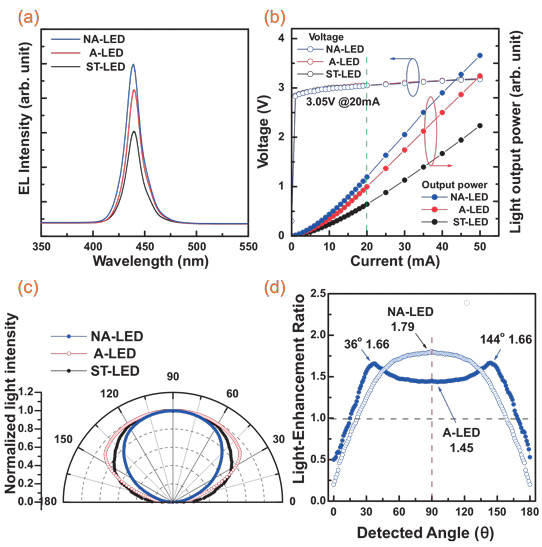
The peak emission wavelength at 20mA for the LED with air-channels and nanoporous regions (NA-LED) was 438.7nm (Figure 2a). The peaks for standard (ST-LED) and air-channel (A-LED) LEDs were both at 439.5nm. The line-widths for all LEDs were around 16nm.

Figure 2: EL emission-peak wavelengths of LEDs measured at 20mA. (b) Operation voltage and light output power versus injection current. (c) Far-field radiation patterns of the LED structures at 20mA. (d) Light-enhancement ratios of A-LED and NA-LED measured by varying detection angle.
The operating voltage at 20mA was also the same over the devices at 3.05V (Figure 2b). However, the NA- and A-LEDs had 1.75x and 1.48x the output power of the ST-LED. The researchers attribute the improvements to better light scattering leading to increased light extraction from the devices.
The air-channels and nanoporosity also led to narrower light beams, with a divergence angle of 122° for the NA-LED, compared with 138° for the A-LED and 146° for the ST-LED (Figure 2c).
http://apex.jsap.jp/link?APEX/6/012103
The author Mike Cooke is a freelance technology journalist who has worked in the semiconductor and advanced technology sectors since 1997.


