- News
12 December 2013
Low-resistivity n-type aluminium gallium nitride for more efficient LEDs
Researchers at Meijo University and Nagoya University, Japan, have produced low-resistance n-type aluminium gallium nitride (n-AlGaN) [Toru Sugiyama et al, Appl. Phys. Express, vol6, p121002, 2013]. Using the n-AlGaN as part of an ultraviolet light-emitting diode (LED), the researchers managed to increase wall-plug efficiency (WPE) by around 15%.
The low-resistance n-AlGaN was produced on sapphire by metal-organic vapor phase epitaxy (MOVPE). The growth began with a low-temperature (LT) buffer layer, followed by a 3μm layer of unintentionally doped GaN. Silane (SiH4) was used as the source for the silicon doping of a 1.5μm AlGaN low-resistivity layer for Hall resistivity and other characterization studies.
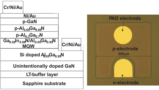
The 390nm violet LED was produced using a similar sample with 2μm n-AlGaN as a base (see Figure 1). The active emitting multiple quantum well (MQW) consisted of three pairs of 2.7nm GaInN wells and 12nm AlGaN barriers. The p-layers of the LED were a 20nm AlGaN electron-blocking layer, a 100nm AlGaN cladding layer and a 10nm GaN contact layer.

Figure 1: Schematic structure and top view of violet LED.
The LED processing consisted of annealing at 800°C in air for 10 minutes to activate the p-type layers, inductively coupled plasma (ICP) mesa etch and deposition of n-type electrode metal, deposition of a nickel-gold semi-transparent electrode on the p-GaN contact, and deposition of the p-type pad electrode. The devices measured 350μm x 350μm.
The researchers found that adding a small amount of aluminium to AlGaN allowed much higher levels of silicon doping to be reached without damaging the crystal structure. Silicon doping in pure GaN is limited to concentrations around 1x10¹⁹/cm3, beyond which the surface of the material becomes rough. By contrast, the AlGaN layers produced in the research were smooth, with no visible cracks even when doped to 4x10²⁰/cm3.
The use of n-AlGaN allows resistivities of 5.9x10⁻⁴/Ω-cm to be reached with carrier concentration of 1.4x10²⁰/cm3 and mobility of 70cm2/V-s. Resistivity reduction in silicon-doped GaN layers saturated around 2.7x10⁻³/Ω-cm with a carrier concentration of 4x10¹⁹/cm3.
Lower-resistivity n-GaN has been achieved by researchers in Germany (Otto-von-Guericke-Universität, TU-Berlin) with germanium doping at 6.3x10⁻⁴Ω-cm. The Meijo/Nagoya n-AlGaN is therefore less resistive than in the Germany-based work.
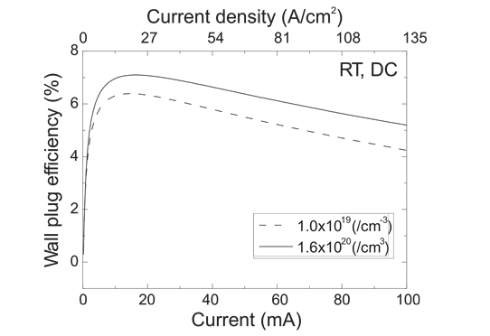
The researchers also compared LEDs with n-AlGaN contact layers with two different levels of silicon doping, giving carrier concentrations of 1x10¹⁹/cm3 and 1.6x10²⁰/cm3. The reduced resistivity of the higher silicon doping was found to reduce the forward voltage for a given drive current, indicating more efficient use of the energy. The reduction was around 1V at 100mA drive current.
There was also a slight increase in light output power for a given drive current. The improvement increased to about 5% at higher currents. The researchers believe that this effect is due to the smaller amount of heat generated by the lower-resistivity n-AlGaN in continuous direct current operation. Droop and overflow effects in the two devices are likely the same due to the similar structure.

Figure 2: WPEs versus injection current.
The improved performance led to a ~15% increase in wall-plug efficiency for the violet LED (Figure 2). The researchers believe that these results could be extended into application in shorter-wavelength devices, including deep ultraviolet (200-300nm) LEDs.
http://apex.jsap.jp/link?APEX/6/121002
The author Mike Cooke is a freelance technology journalist who has worked in the semiconductor and advanced technology sectors since 1997.


