- News
5 August 2013
Nanosphere-patterned sapphire improves deep UV LED performance
Researchers in China have been developing nanopatterned-sapphire substrates (NPSS), achieved with nano-sphere lithography (NSL), as a basis for the production of superior aluminium gallium nitride (AlGaN) semiconductor material for deep ultraviolet (UV) light-emitting diodes (LEDs) [Peng Dong et al, Appl. Phys. Lett., vol102, p241113, 2013].
“We have demonstrated the first high-performance AlGaN-based deep UV-LEDs fabricated on NPSS that is prepared by NSL and wet etching,” says the team from Chinese Academy of Sciences’ Institute of Semiconductors, Tsinghua University, and State Key Laboratory for Artificial Microstructure and Mesoscopic Physics at Peking University
Proposed applications of deep UV LEDs include disinfection, sensing, water purification, bio-medical, and communication. It is also hoped that efficient deep UV LEDs would provide more energy efficient compact solutions compared with the present fragile and hazardous mercury vapor lamps. Improved material quality is key to achieving these aims.
Sapphire patterning was achieved by photolithography through a mask consisting of polystyrene nanospheres that were then removed using deionized water (Figure 1). The pattern in the developed photoresist was transferred to an underlying hard mask layer of 200nm silicon dioxide using inductively coupled plasma etch. Finally, the sapphire was wet etched using a mix of sulfuric and phosphoric acid solutions. The silicon dioxide was removed using hydrofluoric acid.
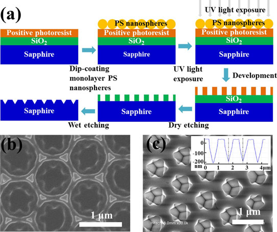
Figure 1. (a) Schematic of fabrication process flow to create nano-patterns on a sapphire substrate (NPSS). SEM images of the patterned photoresist (b) and wet-etched NPSS (c). Inset in Figure 1(c) shows line profile of patterns of NPSS by AFM measurement.
The pattern consisted of 230nm-deep concave triangular cones set in a hexagonal pattern of period 900nm. The unetched region between the cones was 400nm wide.
The growth of the UV LED epitaxial structure was through low-pressure metal-organic chemical vapor deposition (LP-MOCVD) with trimethyl-aluminium, trimethyl-gallium, and ammonia precursors, respectively, for the Al, Ga, and N species. The structure began with 25nm of low-temperature 550°C AlN, before the whole 4μm AlN template was completed at 1200°C in nitrogen-rich conditions.
The AlN was found to coalesce after only 3μm. This is much sooner than other epitaxial layer overgrowth (ELOG) techniques using micro-stripe patterning that only coalesce after 10μm growth. Atomic force microscopy (AFM) over 5μm x 5μm fields gave a root-mean-square roughness of 0.15nm. The AFM analysis also indicated a step-flow growth mode. X-ray analysis gave estimates for screw and edge dislocation densities of 1.6x10⁷/cm2 and 1.2x10⁹/cm2, respectively.
This AlN template material was used in further growth of the UV LED structure (Figure 2). The same structure was grown on flat sapphire with a 1μm AlN template layer. The n-AlGaN layer was found to have pure edge and mixed threading dislocation densities on NPSS and FSS substrates of ~1.6x10⁹/cm2 and ~3.4x10⁹/cm2, respectively. The reduced density layer on NPSS was attributed to the higher-quality AlN template. The superlattice regions were also designed to have dislocation filtering effects.
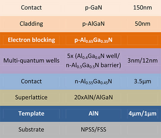
Figure 2. Deep UV LED structure.
Temperature-dependent photoluminescence studies at 10K and 300K suggested an internal quantum efficiency of 45% for the NPSS LED structure, compared with 28% for the FSS AlN template epitaxy.
The epitaxial materials were formed into 380μm x 380μm devices. Mesas for the devices were etched using inductively coupled plasma. The n-contact metal stack consisted of titanium/aluminium/titanium/gold annealed at 850°C in nitrogen. The p-contact was nickel/gold annealed in air at 500°C.
The chips were flip-chip mounted on silicon sub-mounts with gold-bump bonding. The majority of light in deep UV LEDs is expected to emerge through the sapphire substrate, since the p-GaN layer is absorbing of the radiation due to it having the narrowest bandgap in the structure. The device testing was performed with the sub-mounted chips attached to metal-core circuit boards with silver paste to improve heat dissipation.
The main electroluminescence (EL) peak occurred at 282nm with a weak shoulder peak near 330nm (Figure 3). It is thought that recombination in the electron-blocking layer was responsible for the shoulder peak. Hence, “further optimization of the electron-blocking layer is needed to suppress electron overflow into the p-cladding layer,” the researchers write.
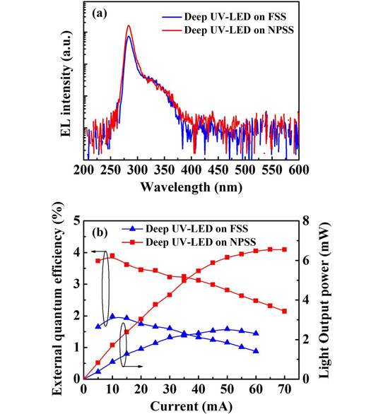
Figure 3. (a) EL spectra and (b) LOP-I-EQE curves of deep UV LEDs grown on NPSS and FSS.
The light output power (LOP) at 20mA current (I) was 3.03mW with external quantum efficiency (EQE) of 3.45% for the NPSS-based device. This was almost double that of the FSS-based LED. The saturation LOP for the NPSS LED was 6.56mW at 60mA current. The FSS device saturated at 2.53mW with 50mA injection.
Since the internal quantum efficiency does not account for all the improvement in performance, the researchers believe that “the light scattering at the AlN/NPSS interface decreases the total internal reflection and the absorption in the p-GaN layer, and increases the photon’s escape opportunity from the sapphire backside.”
DUV LEDs AlGaN LEDs Sapphire substrates
http://link.aip.org/link/doi/10.1063/1.4812237
The author Mike Cooke is a freelance technology journalist who has worked in the semiconductor and advanced technology sectors since 1997.


