- News
5 April 2013
Putting coats on ZnO nanorods for improved light extraction from GaN LEDs
Gwangju Institute of Science and Technology and Samsung Electronics Co Ltd of South Korea have developed a zinc oxide (ZnO) nanorod (NR) process for improving light extraction from gallium nitride (GaN) light-emitting diodes (LEDs) by up to 21% [Chu-Young Cho et al, Appl. Phys. Express, vol6, p042102, 2013].
Light extraction is a problem for GaN-based LEDs because the refractive index of GaN is 2.5, creating a large contrast with that of air (1). The large difference means that light striking a GaN-air interface will be ‘Fresnel reflected’ unless its angle with the normal is less than ~24°.
The Gwangju/Samsung team has developed a process that grows ZnO NRs on indium tin oxide (ITO), a material commonly used as a transparent conductive layer (TCL) for the p-electrode of GaN LEDs.
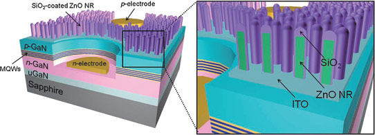
The blue LED structure (Figure 1) was designed to emit at a wavelength of 470nm. The epitaxial material was grown on patterned c-plane sapphire using metal-organic chemical vapor deposition (MOCVD). The patterning consisted of periodic lenses with 3μm diameter and 4μm spacing and 1.5μm height. Patterning of sapphire can improve the crystal structure of epitaxial nitride semiconductor material.

Figure 1: Schematic diagram of blue LEDs with SiO2-coated ZnO NRs on ITO TCL.
The nitride layer sequence consisted of 25nm GaN nucleation (550°C), 2μm n-GaN buffer/contact (1010°C), 5-period 750°C InGaN (3nm) multi-quantum well (MQW) with GaN barriers (12nm), and a 200nm p-GaN contact (980°C).
The 300μm x 300μm LEDs were constructed using inductively coupled plasma (ICP) mesa etch to expose the n-contact layer, deposition of 150nm of indium tin oxide (ITO) as transparent conductive electrode, and deposition of chromium/gold as n- and p-electrode metals.
The ZnO nanorods were seeded by radio-frequency magnetron sputtering a few nanometers of ZnO as a seed layer onto selectively exposed areas of the ITO. The main nanorod growth was carried out by dipping in zinc nitrate hexahydrate (ZnO(NO3)26H2O) and hexamethylenetetramine (C6H12N4) in aqueous solution. The 40nm silicon dioxide (SiO2) coating of the nanorods was achieved through plasma-enhanced chemical vapor deposition (PECVD).
Electron microscopy gave the diameter and height of the nanorods without SiO2 as being ~50nm and ~150nm, respectively. With SiO2 coating, these values increased to ~70nm and ~185nm, respectively. The diameters varied about 20nm each way, and the heights around 10nm.
The ZnO nanorods have a refractive index of 2.08; that of the SiO2 coating is 1.55. The index of ITO is around 2.
Transmittance tests were carried out with ITO/ZnO nanorod structures on glass. At 470nm wavelength, the transmittance without nanorods was 85%. Adding bare nanorods increased this to 90%, and with a SiO2 coating 93% of the light was transmitted.
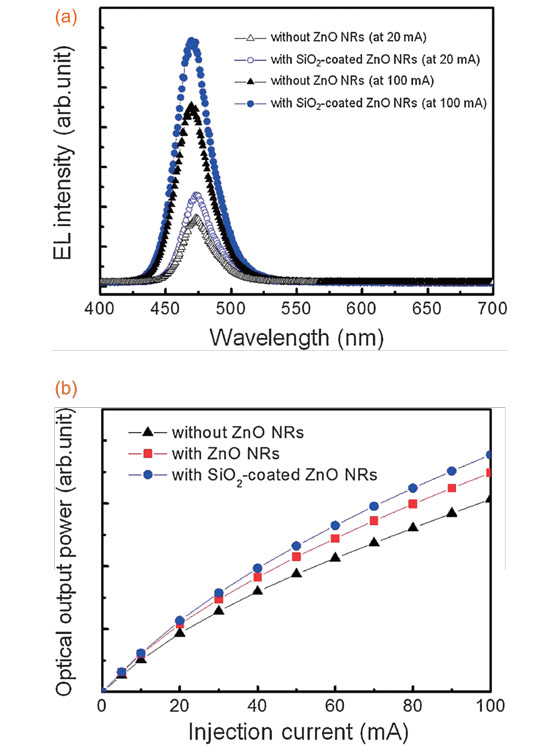
The current-voltage behaviors of LEDs with and without nanorods/coating were very similar. The electroluminescence peak blue-shifts from 472nm to 469nm between 20mA and 100mA current injection (Figure 2). The peak shift is attributed to the “screening effect of the polarization-induced electric field by carriers and to the band-filling effect of the localized energy states formed by the potential fluctuations in MQWs”.

Figure 2: (a) Room-temperature electroluminescence spectra of blue LEDs with and without SiO2-coated ZnO NRs on ITO TCL at injection currents of 20mA and 100mA. (b) Optical output power of LEDs as a function of injection current.
At 20mA, the effect of ZnO nanorods on optical output power was measured as a 15% increase over that of an LED with bare ITO TCL. For the SiO2-coated ZnO nanorods, the improvement was 21% over bare ITO. The percentage increase for SiO2-coated nanorods over bare nanorods was 5% (1.21/1.15-1).
The researchers explain the increased output power with ZnO nanorods as being due to the sub-wavelength surface roughness providing an effective graded refractive index between the ITO layer and air. The SiO2 coating provides a further reduction of the Fresnel reflection effect.
http://apex.jsap.jp/link?APEX/6/042102
The author Mike Cooke is a freelance technology journalist who has worked in the semiconductor and advanced technology sectors since 1997.


