- News
5 November 2012
Quaternary electron emitter injection improves nitride semiconductor LED performance
Researchers in China have improved LED power output and droop behavior in nitride semiconductor light-emitting diodes (LEDs) by including an electron-emitting layer under the active region [Jianbao Zhang et al, Appl. Phys. Express, vol5, p112101, 2012]. The electron-emitting layer included barriers of lattice-matched aluminium indium gallium nitride (AlInGaN) with a view to better controlling electrons in the structure.
The researchers were based at Wuhan National Laboratory for Optoelectronics and Huazhong University of Science and Technology.
Nitride semiconductor LEDs are of much interest for white light applications such as backlights for liquid crystal displays (LCDs) and for general illumination. Presently, these devices suffer from a fall-off (droop) in efficiency at higher currents.
Although the dominant cause of droop is not clear, carrier injection and overshoot problems are found to affect droop. In particular, achieving adequate hole injection into the active region is challenging due to the poor activation of the magnesium acceptor used to create p-type regions in nitride semiconductors. Further, electron/n-type carriers tend to overshoot the active region, recombining non-radiatively in the p-type contact.
One way to avoid overshoot is to include an electron-blocking layer (EBL) of aluminium gallium nitride (AlGaN) before the p-contact layers. Unfortunately, EBLs also tend to reduce hole injection into the active light-emitting region of the device.
Another method to reduce overshoot could be through electron-emitting layers between the n-contact/cladding and active regions that reduce the energy of electrons entering the active region.
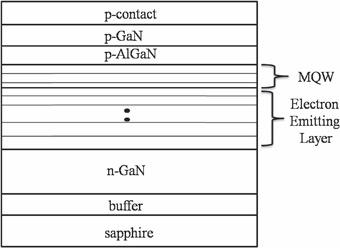
The epitaxial material for the Chinese research (Figure 1) was grown on 2-inch c-plane sapphire substrates using a Veeco K465i metal-organic chemical vapor deposition (MOCVD) system. The multi-quantum well (MQW) structure for the electron emitter consisted of 5 pairs of undoped 1.7nm In0.08Ga0.92N in silicon-doped 16nm n-Al0.12In0.04Ga0.84N barriers. Comparison samples with pure GaN barriers were also produced.
 Figure 1: Schematic structure of LEDs with AlInGaN/InGaN MQW electron-emitting layer.
At room temperature, the lattice constant of a free-standing layer of AlInGaN (3.1878Å) with the given composition is close to that of GaN (3.1820Å). So the lattice mismatch between the barriers and wells of the emitter region is similar in the two cases. The difference is that the AlInGaN presents a higher energy barrier with a larger bandgap offset of about 0.1eV.
The active light-emitting MQW region consisted of 12 pairs of 2.8nm undoped In0.21Ga0.79N and 14nm silicon-doped n-GaN barriers. Further layers of p-AlGaN for electron blocking and two layers of p-GaN for the contact region completed the structure. Also, an epitaxial structure for an LED without an electron-emitter region was also produced for a comparison with conventional LED performance.
The LEDs were produced in a standard process (contact metal, mesa isolation, etc) with thinning of the sapphire substrate to about 90μm and dicing into 300μm squares. Bare chips were tested.
One effect of using AlInGaN in the electron emitter is to reduce the forward voltage, indicating smaller power loss at a given current. This effect is attributed to the better current spreading due to the MQWs trapping electrons before injection by tunneling into the active region. The barrier of AlInGaN is higher than that of pure GaN, increasing the trapping effect.
Further, the leakage under reverse bias was reduced. At –30V, the leakage without emitter layer is 21.70μA, while devices with emitter layers leak 7.82μA when the barriers are GaN and 3.24μA with AlinGaN barriers. These results suggested to the researchers that the reduced leakage for the LEDs with electron-emitter layers reflect lower dislocation densities in these samples.
Atomic force microscopy (AFM) on epitaxial samples without p-type layers confirmed this, giving pit densities of 3.22x10⁸/cm2 for samples without electron emitters, 2.62x10⁸/cm2 for material with electron emitters with GaN barriers, and 1.87x10⁸/cm2 for the new material with AlInGaN barriers in the electron emitters.
The superlattice MQW structure is thought to block/filter dislocations from threading through from the buffer to active layers. The superlattice AlInGaN is apparently better at this than SLs with GaN barriers. The diameter of the pits is also smaller for AlInGaN barriers (~95nm) than for the other samples (~125nm).
The researchers comment: “It seems that the adoption of Al0.12In0.04Ga0.84N/In0.08Ga0.92N MQW electron-emitting layer can greatly delay the formation of pits, leading to smaller pit sizes. More investigations are needed to understand this issue.”
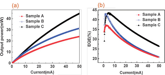
The emission peak for electroluminescence was at 457.5nm at 20mA current injection. The LED with AlInGaN barrier electron emitter also had the highest output power and peak external quantum efficiency (Figure 2). Further, the fall-off of EQE for higher currents was slower.

Figure 2: (a) Output power vs current (L–I) characteristics and (b) plot of EQE as a function of current for samples A, B, and C, representing LEDs without electron emitter, and with GaN- and AlInGaN-barrier electron emitters, respectively.
Often, measures designed to reduce droop effects end up reducing peak efficiency as well.
The output power at 20mA was 13.2mW, 17.3mW and 21.8mW for the LEDs without electron emitter, and with GaN- and AlInGaN-barrier electron emitters, respectively. The respective peak EQEs were ~37%, ~42% (at 2mA) and 42% (at 5mA).
The researcher suggest that their results could be “mainly due to the fact that the higher bandgap of AlInGaN barrier, as compared with that of the GaN barrier, can more effectively slow down the electron velocity in the vertical direction and force more electrons to transport laterally, and thus simultaneously improve the carrier confinement in the MQW active region and the current spreading especially for the high-injection-current case.”
It was also found that the AlInGaN electron emitter gave better electrostatic discharge (ESD) endurance – while the other LEDs almost completely failed under 5000V stress, 70% of the AlInGaN devices passed the test. The researchers attribute the improved ESD performance to reduced numbers of dislocations in the active region.
LEDs LED droop GaN AlInGaN MOCVD
http://apex.jsap.jp/link?APEX/5/112101
The author Mike Cooke is a freelance technology journalist who has worked in the semiconductor and advanced technology sectors since 1997.


