- News
29 November 2012
First 268nm DUV LEDs on AlN substrate
Researchers from Japan and the USA have reported the first fabrication on hydride vapor phase epitaxy (HVPE) aluminium nitride (AlN) substrates of aluminium gallium nitride (AlGaN) light-emitting diodes (LEDs) that emit at the deep-ultraviolet (DUV) wavelength of 268nm [Toru Kinoshita et al, Appl. Phys. Express, vol5, p122101, 2012].
The Japanese organizations involved were Tokuyama Corp, Kobe University, Tokyo University of Agriculture and Technology, and the National Institute of Information and Communications Technology. They were joined by US company HexaTech Inc and North Carolina State University.
There is much interest in shrinking the wavelength of AlGaN LED emissions to the DUV range around 265nm for air and water purification. This range is an absorption maximum for DNA, and hence 265nm DUV can be used to disrupt biological agents such as bacteria. UV-based purification presently depends on costly, bulky mercury lamp systems. The breakage of such lamps can also result in toxic mercury pollution.
Most work on AlGaN LEDs for this wavelength range is carried out on sapphire substrates. However, large lattice mismatches lead to dislocations in the active material region that emits the light, reducing energy efficiency to a couple of percent.
The Japan/US team hopes that developing AlGaN LEDs on AlN will reduce the mismatch and lead to more efficient devices.
HVPE was used to grown thick 250μm AlN layers on c-plane physical vapor transport (PVT) AlN substrates. Chemical mechanical polishing (CMP) was used to prepare the HVPE AlN surface for the subsequent epitaxy of the LED structure. After CMP, the root-mean-square surface roughness was less than 0.2nm.
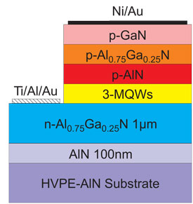
The device layers were grown using metal-organic chemical vapor deposition (MOCVD) in an Aixtron AIX200/4RF-S reactor (Figure 1). The active region consisted of a three-period multi-quantum well (MQW). The p-type layers were an AlN electron-block layer, an AlGaN cladding layer, and a GaN contact layer. Although GaN absorbs DUV, the researchers felt that it was needed to provide a suitable ohmic contact with the nickel/gold p-electrode. Unfortunately, p-type doping becomes even more difficult as the aluminium content of AlGaN is increased.
 Figure 1: Schematic structure of a 268nm DUV-LED.
X-ray analysis showed that the layers of the device were strained pseudomorpically to the underlying AlN, except for the final p-GaN, which was almost completely relaxed due to the large lattice mismatch.
The 400μm x 600μm LED devices were produced using photolithography, dry etching, and metal evaporation. The PVT-AlN was removed using mechanical polishing to reduce the amount of DUV absorption. Some of the HVPE-AlN was also removed, and the researchers estimate that the thickness of this layer after polishing was 170μm.
Fortunately, the HVPE-AlN absorbed far less of the 265nm-wavelength radiation than does the PVT-AlN substrate. Below 300nm wavelengths, the transmittance of the PVT-AlN substrate was effectively zero. By contrast, the HVPE-AlN allowed as much as 62% of the 265nm radiation through. “This value is close to the ideal value when surface reflection is taken into account,” the researchers comment. The intrinsic absorption of HVPE-AlN was measured at 10/cm for 265nm UV.
Without removal of the PVT-AlN, LEDs produced little external radiation and none detectable below 300nm. Weak peaks at 320nm and 450nm were attributed to photoluminescence in the PVT-AlN excited by the DUV from the MQW.
Reduction in light absorbance is important since nitride semiconductor UV LEDs are generally operated in a flipped orientation, with the light being extracted through the growth substrate. This is because p-GaN contact layers heavily absorb DUV that has higher energy than the GaN bandgap.
The individual LED chips were flipped onto sintered AlN submounts and attached with gold-tin solder bumps. This assembly was then glued into a 1mm x 0.5mm AlN carrier with silver paste.
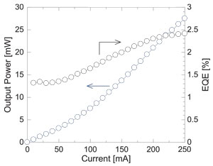
 Figure 2: Output power and EQE of flip-chip-mounted DUV-LED as function of injection current.
Electroluminescence spectra showed a main peak at 268nm and a weak parasitic peak around 300nm. “This peak is likely to be due to the recombination from the conduction band to the deep acceptor level in the p-Al0.75Ga0.25N cladding layer,” the researchers comment.
The continuous-wave output power was 28mW at 250mA, with external quantum efficiency (EQE) of 2.4% (Figure 2). A super-linear increase in output power and increase in EQE with injection current is attributed to thermal activation of the p-type layers from self-heating effects.
DUV LEDs AlGaN LEDs AlN substrates HVPE
http://apex.jsap.jp/link?APEX/5/122101
The author Mike Cooke is a freelance technology journalist who has worked in the semiconductor and advanced technology sectors since 1997.


