- News
31 May 2012
Annealing RIE damage to improve InGaAs QWFET performance
Massachusetts Institute of Technology (MIT) researchers have found that a post-etch anneal dramatically improves the performance of their self-aligned indium gallium arsenide (InGaAs) quantum-well metal–oxide–semiconductor field-effect transistors (QWFETs) [Jianqiang Lin et al, Appl. Phys. Express vol5, p064002, 2012].
 It is hoped that devices with high-mobility channels such as InGaAs could lead to higher-performance logic than traditional silicon-based CMOS circuitry. However, developing manufacturable self-aligned processes involving anisotropic etching is a challenge to researchers. For InGaAs devices, a particular concern is that such anisotropic reactive-ion etching (RIE) can severely damage device performance.
The MIT devices were produced from lattice-matched epitaxial heterostructures grown by molecular beam epitaxy (MBE) wafer supplier IntelliEpi Inc on indium phosphide (InP) substrates with 400nm InAlAs buffer, 15nm InGaAs channel, 4nm InP etch stop, and 15nm n-InGaAs cap layers. The InAlAs layer was Si-doped in a thin layer at 5nm beneath the channel.
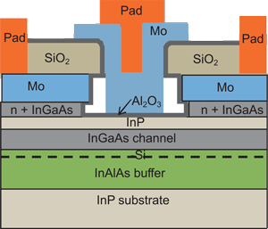
Figure 1: Cross-sectional schematic of self-aligned InGaAs QW-MOSFET. A self-aligned air spacer that is passivated by Al2O3 separates the S/D and gate metal. The side recess length is 100nm.
Device fabrication (Figure 1) was carried out at the Microsystems Technology Laboratories at MIT. The first step was to evaporate 50nm molybdenum (Mo), then apply 60nm silicon dioxide (SiO2) through plasma-enhanced chemical vapor deposition (PECVD).
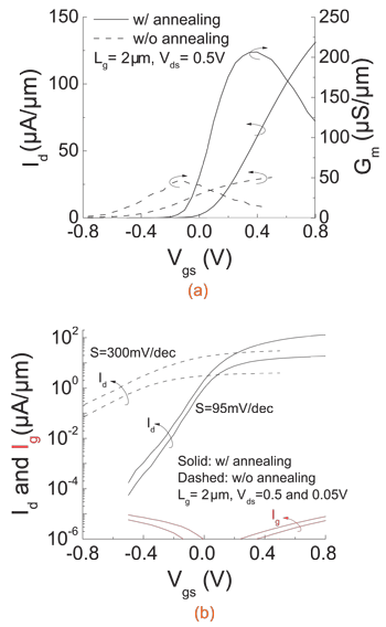
 Figure 2: (a) Transfer and transconductance characteristics of QW-MOSFET with (solid) and without (dashed) RIE damage annealing. (b) Subthreshold characteristics and gate leakage current of QW-MOSFET with (solid) and without (dashed) RIE damage annealing.
The gate region was defined using photolithography and then a series of etches carried out to reach the InP etch stop layer. These RIEs were followed by a selective plasma etch designed to pull back the Mo from the edges of the SiO2 layer. The RIE damage was repaired using a 340°C anneal in nitrogen for 15 minutes. The InGaAs cap layer was etched under the Mo layer using a wet etch of citric acid in hydrogen peroxide.
Cleaning and thinning of the InP layer was then performed before the application of 4nm Al2O3 dielectric using atomic layer deposition (ALD). More Mo was then applied and etched as gate metal. The element was chosen because it is CMOS-compatible, has a suitable workfunction and, further, it can be patterned using RIE.
The RIE damage annealing produced dramatic improvements in 2μm-gate-length devices (Figure 2). The peak transconductance was increased from around 50μS/μm for a non-annealed device to 205μS/μm with annealing. The subthreshold swing was reduced from 300mV/dec to 95mV/dec.
The threshold voltage of the annealed device was negative at -37mV, but was closer to the enhancement-mode region (> 0V) needed for CMOS logic applications. Also, the gate leakage at 1V overdrive potential was low, at 1.1x10⁻⁴A/cm2.
InGaAs QWFET InGaAs Annealing RIE MBE PECVD ALD IntelliEpi InP substrates
The author Mike Cooke is a freelance technology journalist who has worked in the semiconductor and advanced technology sectors since 1997.
