- News
8 May 2012
Electrical efficiency and current crowding in vertical InGaN/SiC LEDs
Researchers at Ukraine’s Lashkaryov Institute of Semiconductor Physics have been studying current crowding and electrical efficiency degradation in vertical indium gallium nitride (InGaN) light-emitting diodes(LEDs) made from material grown on silicon carbide (SiC) substrates [Volodimir K. Malyutenko et al, IEEE Photonics Technology Letters, published online 25 April 2012].
The researchers stress the importance of power conversion efficiency (PCE) – the ratio of output to input – as the key figure of merit for LEDs. Degradation effects for PCE include optical losses from non-radiative recombination and poor light extraction and electrical losses such as shunt and series resistances from contact metals and thick device layers.
The team was particularly keen to seek out the ways in which the PCE of high-power devices could be improved. SiC is an interesting substrate for such devices since it has high thermal conductivity and can be made in an electrically conducting form. This is in contrast to the main commercial substrate for nitride semiconductor light-emitting devices – sapphire – which is both thermally and electrically insulating.
The use of an electrically conducting substrate allows for vertical current flow through the device, which reduces the operating voltage and series resistance, improves current spreading and thermal management, and allows for a wider light-emitting area. Sapphire substrate devices must have their two electrical contacts on the same side of the device, with the current needing to flow laterally to reach the active region.
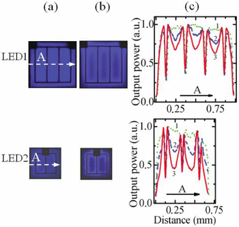
 The researchers used commercial 475mm blue InGaN multi-quantum well LED epitaxial structures grown on conductive silicon carbide (SiC) substrates. The use of conducting SiC allows vertical LED structures. The Lashkaryov researchers applied a continuous metal electrode to the p-contact and two types of grid pattern (Figure 1) to the n-contact to allow light extraction. The junction areas of the LEDs were square, of sides 950μm (LED1) and 650μm (LED2). The LED1 grid had three loops separated by 225μm, while the two-loop LED2 had 200μm separations. The contact stripes of LED1 were twice as long as LED2’s.
Figure 1: Summary of the optical characterization of LEDs. Near-field maps of light escaping devices at (a) 1mA current, and (b) maximum rated current; (c) shows light profiles in LEDs along the line A at (1) 1mA, (2) 0.5A, and (3) maximum rated current.
The maximum rated pulsed forward currents of LED1 and LED2 were 1.25A and 1.0A, respectively. The researchers found that these currents fall in the domain where the series resistance losses of the devices are significant. The series resistances of the devices were similar at 0.83Ω (LED1) and 1.15Ω (LED2), despite LED1 having twice the area of LED2. At the maximum rated currents, the researchers estimate that around 25% of the input power in either device was lost due to series resistance.
The LEDs were soldered p-side down to a massive heat sink. Measurements were carried out at room temperature using pulsed currents to avoid self-heating effects.
Near-field light-emission profiles were gathered by scans across the devices with an optical microscope and measurement by CCD (Figure 1c). As the current increases to the maximum rating value, the LED emissions are seen to be more concentrated near the electrodes due to current-crowding effects. At the maximum current, light emission in the center of the loops is only 60% of maximum for LED1 and 45% for LED2. The researchers estimate that the current-spreading lengths from the electrode at maximum current are 90μm and 60μm for LED1 and LED2, respectively.
 Since the light emission in the electrode-free region is much reduced, these current-crowding effects lead to more light being blocked by the n-contact. The effective emitting region is therefore much smaller than the active device area. The result is degradation of both internal quantum efficiency (IQE) and external quantum efficiency (EQE).
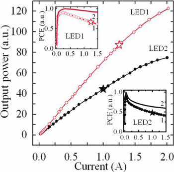
Figure 2: Experimental light output power versus current. Both curves are normalized to the light intensity at 20mA. Insets: power conversion efficiency as (1) a function of current calculated for the input power and (2) the power consumed by the junction.
The researchers comment: “Such observations coincide well with the results of previous studies performed on vertical AlGaInP, AlGaAs and InAsSbP LEDs, and demonstrate the critical need for developing a current-crowding-free vertical design for high-power LEDs.”
The researchers also carried out total light output power measurements as functions of injection current to determine the effects of series resistance on performance. The behavior of the power conversion efficiency showed a typical droop effect at high current. The PCE fall from maximum light output (at 340mA for LED1 and 43mA for LED2) to that at the maximum rated current was 26% for LED1 and 48% for LED2. Removing the losses from series resistance reduced these falls to 10% for LED1 and 37% for LED2.
The researchers believe that efforts to improve light extraction (involving roughening the emission surfaces to reduce reflection of light back into devices) could significantly increase series resistance, enhance current-crowding effects, and reduce the current spreading length. “All these could impair the benefit in optical power emitted at given current by decreasing the electrical efficiency and PCE through the need to increase both voltage and input power,” they say.
Vertical InGaN/SiC LEDs SiC substrates
The author Mike Cooke is a freelance technology journalist who has worked in the semiconductor and advanced technology sectors since 1997.
