- News
23 January 2012
Honeycomb sweetens nitride solar cell performance
Taiwan researchers have been using silicon dioxide (SiO2) honeycomb structures to increase the performance of nitride semiconductor solar cells [P. H. Fu et al, Appl. Phys. Lett., vol100, p013105, 2012]. The research was carried out by participants from National Taiwan University, Genesis Photonics Inc, and National Central University.
The honeycomb structure reduces the amount of light reflected from the cell’s top surface, hopefully allowing more light to enter into the active region and creating more electrical power. Performance under simulated 1.5 air-mass (AM1.5G) solar illumination showed 7% increased short-circuit current density (Jsc) over a bare comparison device (Table 1). The open-circuit voltage (Voc) was the same in the two devices. The energy conversion efficiency is boosted by some 34%, thanks both to the increased current and an enhanced fill factor (maximum converted power/(VocxIsc)).
AR layers |
Bare surfaces |
Nano-honeycombs |
Voc (V) |
1.9 |
1.9 |
Jsc (mA/cm2) |
0.84 |
0.90 |
Fill factor (%) |
25.94 |
32.23 |
Energy conversion (%) |
0.41 |
0.55* |
Table 1: Photovoltaic characteristics of the MQW solar cells with bare surfaces and nano-honeycombs.
*Actually there is a slight error in Table 1, as published in Appl. Phys. Lett. Using the given values of Voc, Jsc, fill factor, and standard test condition solar power of 1000W/m2, one gets a higher value of 0.55% for the conversion efficiency, rather than the published value of 0.51. This has been confirmed with the corresponding author.
The values of the conversion efficiency are less than 1% because the peak wavelength of the device for energy conversion is somewhat shorter (380nm) than that of the incident solar radiation (~500nm).
The epitaxial material for the Taiwan device was grown on c-plane sapphire using metal-organic chemical vapor deposition (MOCVD). The undoped active layer consisted of a 9-period multi-quantum well structure of 3nm indium gallium nitride (In0.3Ga0.7N) wells separated by 17nm GaN barriers. The n-type layer was 2.5μm and the p-type layer was 0.2μm.
The device was formed from this material by first depositing an indium tin oxide (ITO) transparent conductive layer on the p-GaN contact layer, etching 1mm x 1mm of LED mesas, and deposition of titanium/aluminum/nickel/gold contacts. The p-metal was patterned in an interdigitated grid format, either deposited on the bare ITO or on the nano-honeycomb.
The nano-honeycomb was produced by depositing 450nm of SiO2 by electron-beam evaporation. A 5-minute oxygen plasma treatment made the surface hydrophilic. Polystyrene 450nm-diameter spheres in deionized water were then coated onto the SiO2 to serve as an etch mask. The wafer was then put in an incubator at 50°C/87.5% humidity for two hours. This resulted in a close-packed monolayer of spheres. To create gaps between the spheres, they were next subjected to oxygen plasma. This was followed by trifluoromethane to etch the SiO2. Further oxygen plasma was used to remove the nano-sphere residue.

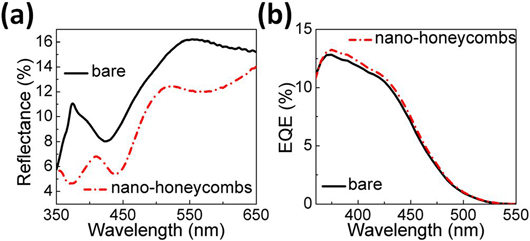
Figure 1: (a) Specular reflectance and (b) EQEs measured on the MQW solar cells with bare surface and SiO2 honeycombs.
The effect of the SiO2 structure is to reduce reflection that blocks sunlight from entering the device (Figure 1). One aspect of this is that the SiO2 has a refractive index intermediate between that of air (1) and the ITO (2.04 at 500nm wavelength). The external quantum efficiency (EQE) measured under monochromatic illumination from a halogen lamp is thus enhanced by several percent. The peak wavelength is 380nm in both cases. Simulations suggest that the honeycomb structuring broadens the light intensity distribution within the device through scattering.
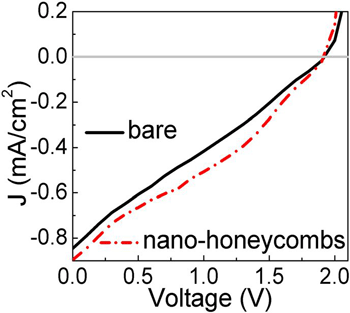
 The increased slope of the current–voltage curve (Figure 2) with honeycomb structure under AM1.5G illumination indicates reduced series resistance, and thus a larger fill factor.
Figure 2: Current density–voltage (J–V) characteristics measured on MQW solar cells with bare surface and nano-honeycombs.
The leader of the team, Jr-Hau (JH) He, comments: “Since the fabrication process of SiO2 honeycombs does not induce any damage to the internal device structures, the increased fill factor can be mainly attributed to the improved quality of the SiO2/ITO interface. Due to the dielectric properties of SiO2, the photo-generated carriers are more likely to be collected by the electrodes by the path inside the device (under ITO/GaN interface) instead of trapped by surface defects at the ITO surface.”
AlN interlayer doubles conversion of nitride semiconductor solar cell
Improving PV material quality with patterned sapphire
Superlattice nitride solar cells achieve higher conversion
Nitride solar cell achieves peak EQE of 72%
www.g-photonics.com/ENG/index.htm
The author Mike Cooke is a freelance technology journalist who has worked in the semiconductor and advanced technology sectors since 1997.
