- News
15 February 2012
Nano-textured ITO improves light extraction in nitride LEDs
Researchers in China have used self-assembled cesium chloride (CsCl) nanospheres as a cost-effective mask for nano-texturing indium tin oxide (ITO) transparent conducting layers on nitride semiconductor light-emitting diodes (LEDs) to improve light extraction by up to 23.4% [Yiyun Zhang et al, Jpn. J. Appl. Phys., vol51, p020204, 2012].
The researchers were based at the Chinese Academy of Sciences’ institutes of semiconductors (Semiconductor Lighting Technology Research and Development Center) and of high-energy physics in Beijing. Researchers from the same facilities had previously attempted to use CsCl nanospheres to nano-texture the p-type gallium nitride (GaN) layer of nitride LEDs directly, but found that the process often degraded the electrical performance of the devices.
The purpose of such texturing is to reduce the amount of light reflected back into the LED at interfaces between materials with different refractive indices, such as GaN/air or ITO/air.
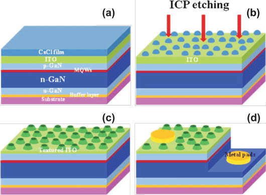
In the new work, conventional LED structures were grown on sapphire using metal-organic chemical vapor deposition (MOCVD) – see Figure 1. The active layer consisted of an 8-period multi-quantum well (MQW) with InGaN wells and GaN barriers.

Figure 1: Schematics of fabrication process: (a) CsCl film deposition, (b) ICP etching, (c) nanoislands on the ITO layer, and (d) metal pad fabrication.
A 300nm indium tin oxide (ITO) transparent conducting layer was electron-beam deposited on the top p-GaN layer of the LED. This was followed by thermal evaporation of cesium chloride (CsCl) onto the ITO – various thicknesses of this layer were tested to optimize the process.
Exposure of the CsCl layer to water vapor caused the material to ‘self-assemble’ into ‘nanospheres’. The spheres were randomly distributed on the wafer surface (1.6-0.13x10⁹/cm2). The average diameter of the spheres (450-900nm) is controlled by the CsCl film thickness (50-150nm), relative humidity, and development time. In fact, the ‘spheres’ were not spherical but rather approximately hemispherical – a 700nm-wide island had a height of about 300nm.
The wafer was then subjected to inductively coupled plasma etching to pattern the ITO surface. The CsCl residue was then removed by soaking in deionized water. This etch process textured the ITO surface into truncated-cone nanoislands.
LEDs were constructed from the resulting material by etching mesas and applying chromium/platinum/gold metal layers on the p- and n-type contact layers.
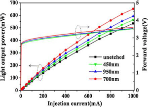
 All the treated ITO surfaces showed improved light output power at 350mA over a planar device (Figure 2). The largest improvement of 23.4% came from the 700nm nanosphere etched surface. The improvements for the 450nm and 900nm nanosphere treatments were 6.8% and 13.1%, respectively.
Figure 2: Light output power and forward voltage versus current for LEDs produced using different CsCl nanosphere sizes.
The researchers comment: “Obviously, there is an optimal size of the cesium chloride nanospheres. When the cesium chloride nanospheres are too large, the light scattering occurring at the interface between the ITO layer and the air will be reduced because of the fewer nanoislands fabricated on the ITO layer. On the other hand, too small cesium chloride nanospheres cannot entirely cover the ITO layer, which strongly affects the surface morphology of the etched ITO layer.
There was also an effect of etch time on light output performance, with the maximum coming from a 500sec process.
An important further consideration is that the treatment has little impact on electrical performance, as seen in the very similar current-voltage curves (Figure 2). This allows the researchers to conclude that the electrical performance of the LEDs is not damaged by the etch process. However, there is a slight increase in forward voltage of 0.1V in the best light output power device from 700nm nanospheres. This could be due to the surface being too rough to form good ohmic contacts on the ITO layer.
ITO transparent conducting layers GaN LEDs MOCVD
The author Mike Cooke is a freelance technology journalist who has worked in the semiconductor and advanced technology sectors since 1997.

