- News
4 December 2012
KLA-Tencor launches ICOS WI-2280 fourth-generation wafer inspector for LED and adjacent markets
Process control and yield management solutions provider KLA-Tencor Corp of Milpitas, CA, USA has launched its next-generation LED patterned wafer inspection tool. Designed specifically for defect inspection and 2D metrology for LED applications, the ICOS WI-2280 can also provide enhanced inspection capabilities and increased flexibility for micro-electro-mechanical systems (MEMS) and semiconductor wafers spanning 2-inches to 8-inches in size.

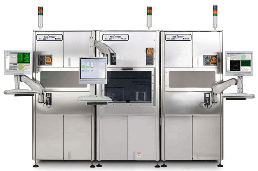
Picture: KLA-Tencor’s new ICOS WI-2280 system.
Built on its WI-22xx platform, the ICOS WI-2280 represents KLA-Tencor’s fourth-generation LED wafer inspection system, delivering sensitivity with increased throughput for reduced cost of ownership. Additionally, the tool supports the handling of whole wafers in carriers and diced wafers in hoop ring or film frame carriers to accommodate multiple media with minimal equipment changeover time. The new system also features an enhanced rule-based binning defect classification and recipe qualification engine, enabling faster yield learning during production ramps, as well as improved process control and process tool monitoring strategies.
“Increasingly, LED manufacturers are demanding improved detection and classification of yield-relevant defects of interest, which enables them to take faster corrective actions to improve their yields at higher inspection throughput,” says Jeff Donnelly, group vice president, Growth and Emerging Markets (GEM) at KLA-Tencor. “There is also a growing need to boost productivity by enabling faster production recipe creation,” he adds. “The ICOS WI-2280 addresses critical market requirements — ultimately enabling LED manufacturers to achieve better lumens per watt and lumens per dollar performance.”
Building on the performance of the ICOS WI range, the WI-2280 includes:
- highly flexible optical modes with dedicated image processing, enabling a high defect capture rate and recipe robustness against a varying process background;
- unique defect classification, delivering faster time to information;
- an advanced recipe tuning engine with best known methods, allowing faster recipe qualification;
- enhanced metrology capability, offering additional yield-relevant actionable data with no impact to throughput;
- front-end to back-end-of-line connectivity analysis capability, delivering a single platform for defect source analysis; and
- an easy-to-use inline or offline reclassification engine, enabling post-inspection yield improvements for enhanced productivity.
In addition to LED application environments, MEMS, semiconductor, compound semiconductor and power device markets can leverage the WI-2280 tool for: back-end-of-line and post-dicing outgoing quality control or binning; front-end-of-line patterned wafer inspection for baseline yield improvement, rework, excursion control or overlay; and 2D surface inspection and metrology.
As part of KLA-Tencor’s LED portfolio, the ICOS WI-2280 works in conjunction with the firm’s Candela LED unpatterned wafer inspection system and Klarity LED automated analysis and defect data management system, providing comprehensive end-to-end inspection coverage.
All tools are backed by KLA-Tencor’s global, comprehensive service network.
KLA-Tencor LEDs ICOS Inspection


