- News
3 April 2012
Improving InGaN channel for HEMT power amp/switching apps
Epiwafer foundry Kopin Corp of Taunton, MA, USA and University of Notre Dame (UND) have developed record high-mobility indium gallium nitride (InGaN) channel layers in high-electron-mobility transistor (HEMT)-type epitaxial structures [O. Laboutin et al, Appl. Phys. Lett., vol100, p121909, 2012]. Kopin sees potential for improving the performance of next-generation power amplifiers and power switching converters.
The researchers are seeking ways to produce ultra-high-frequency operation through reduced-scale components. In particular, they want to reduce gate lengths and barrier thickness without short-channel effects that degrade performance.
Presently, nitride semiconductor HEMTs tend to use GaN channel layers but, as transistor dimensions reduce, such channels suffer from reduced electron densities due to the reduced polarization effect from thinner barriers.
Improvements have been seen from the use of aluminium indium nitride (AlInN) as opposed to aluminium gallium nitride (AlGaN) barriers. Also, the use of a back-barrier underneath the channel can better confine the conduction electrons, boosting short-channel performance. However, producing high-quality structures with appropriate polarization fields to achieve this is a challenge.
An alternative is to use a narrower-bandgap material between the barrier and buffer that would naturally confine electrons. InGaN is such a narrow-bandgap material. However, InGaN is notoriously difficult to grow with smooth interfaces and uniform alloy composition.
The Kopin/UND HEMT epitaxial structures (Table 1) were produced in a close-coupled showerhead metal-organic chemical vapor deposition (MOCVD) reactor operating at low pressure on sapphire and silicon carbide (SiC). The optimized AlInGaN/AlN composite barrier was reported in the last year by researchers from Kopin, UND, and University of Florida.
AlInGaN/AlN |
Composite barrier |
11nm |
750°C |
InGaN |
Channel |
5-9nm |
710-790°C |
GaN |
Buffer |
1.9μm |
|
GaN or AlN |
Nucleation |
|
|
Table 1: HEMT structure explored by Kopin/UND research.
During development of the new InGaN channel structure, the effect of increasing the growth temperature was studied. For an InGaN layer with 6% In molar fraction, an increasing trimethyl-indium flux of 1.5 up to 25μmol/min was needed as the growth temperature increased from 710°C to 790°C. At the same time, the trimethyl-gallium flux was decreased from 18μmol/min to 6μmol/min, reducing the growth rate from 0.08nm/s to 0.03nm/s.
It was found that higher-temperature, lower-growth-rate deposition resulted in improved characteristics. In particular, root-mean-square surface roughness decreased from 0.8nm for 710°C growth to 0.5nm at 790°C. Such a reduction in roughness should lead to reduced interface scattering and hence improved mobility.
Photoluminescence experiments also suggest improved uniformity of the InGaN alloy. In particular, the InGaN peak is reduced in the lower-growth-rate, high-temperature sample. A large InGaN peak can be indicative of carrier localization at non-uniformities in alloy composition.
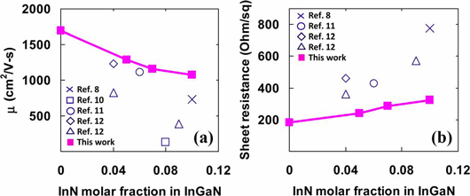
Using the low-growth-rate and high-temperature deposition process, full HEMT structures with InGaN channels with varying In composition in the range 0-10% were produced on silicon carbide and characterized (Figure 1). The mobility varied from 1690cm2/V-s for pure GaN down to 1070cm2/V-s for 10%-In InGaN channels. Such a decreasing trend is also observed in structures with more traditional AlGaN barriers.

Figure 1: Electron mobility and sheet resistance as functions of InxGa1-xN channel composition for full HEMT structures. Further data points from literature with AlGaN and InGaN barriers and channel carrier concentrations include, respectively, Al0.25Ga0.75N and 1.1x10¹³/cm2 (Ref. 8), Al0.33Ga0.67N and 1.5x10¹³/cm2 (Ref. 10), Al0.3Ga0.7N and 1.3x10¹³/cm2 (Ref. 11), for Al0.24In0.01Ga0.75N and 1.1x10¹³/cm2 (Ref. 12), Al0.83In0.17N and 2.1 2.8x10¹³/cm2 (Ref. 12).
The researchers point out that despite the increased sheet charge (~2x10¹³/cm2), which is often associated with reduced mobility, “the electron mobility was higher than that in the AlGaN structures within the entire InxGa1-xN compositional range.”
For the 5%-In sample, the record 1290cm2/V-s value produced an average sheet resistance value of 240Ω/square (~30% lower than the previous best published result for InGaN channels) with standard deviation of 4.2% across the 3-inch sample.
The work at Kopin was partially supported by the US Missile Defense Agency (MDA) via Small-Business Innovation Research (SBIR) funding.
Kopin InGaN channel Nitride HEMT
http://link.aip.org/link/doi/10.1063/1.3697415
The author Mike Cooke is a freelance technology journalist who has worked in the semiconductor and advanced technology sectors since 1997.
