- News
4 April 2012
FBH reports high-speed InP HBTs using transferred-substrate technology
 At the 7th German Microwave Conference (GeMiC 2012) in Ilmenau, Germany recently (12–14 March), Berlin-based Ferdinand-Braun-Institut, Leibniz-Institut für Höchstfrequenztechnik (FBH) reported how it has established a transferred substrate (TS) technology to optimize the high-frequency and power performance of InP/InGaAs/InP double-heterojunction bipolar transistors (DHBTs) – see T. Al-Sawaf et al, ‘W-Band Amplifier with 8dB Gain Based on InPHBT Transferred-Substrate Technology’, Proc. German Microwave Conference, paper 1474.
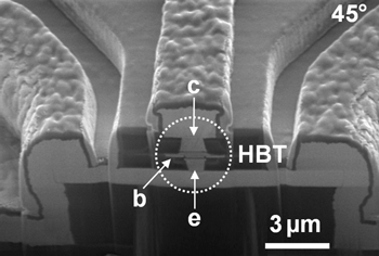
Figure 1: Focused ion beam (FIB) cross section of a TS-HBT, showing emitter (e), base (b) and collector (c).
Research on high-speed transistors is driven by applications for imaging and wide band communications, says FBH. Recent technical advances in InP-based transistors with operating frequencies of several hundred gigahertz (GHz) - together with their outstanding material properties - qualify them as key components in such systems, it adds.
FBH’s latest 3” wafer-level process enables lithographic access to both the HBT’s front-side and back-side, aligned to each other. The resulting linear device (shown in Figure 1) eliminates dominant transistor parasitics and relaxes design trade-offs.
 The essential step for gaining access to both sides of the epitaxial structure is to completely remove the supporting substrate. FBH hence developed a robust adhesive wafer bonding procedure via benzocyclobutene (BCB). This yields a homogenous, crack- and void-free composite matrix of transistors transferred on the wafer-level scale.
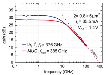
Figure 2: Extrapolated fT and fmax of a TS-HBT.
The optimized device topology of the two-finger transistor has a total emitter area of 2× 0.8μm ×5μm (as depicted in Figure 2). This yielded a current-gain cut-off frequency (fT ) of 376GHz and a maximum oscillation frequency (fmax) of 385GHz at breakdown voltages (BVCEO) of more than 4.5V. The InP HBTs combine high-frequency performance with saturated output power (Pout) of more than 14.2dBm @77GHz and an inherently good matching to 50Ω. FBH says that the highly scalable device architecture is capable of even further increases in frequency as well as power performance in the future.
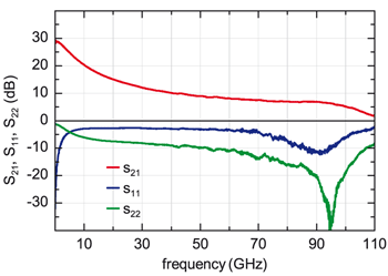
 Single-stage power amplifiers have been designed and realized in TS technology for 90GHz operation. Their S-parameter measurements (shown in Figure 3) confirm good agreement with modeling.
Figure 3: S-parameter measurements of 90GHz power amplifier in TS technology.
FBH notes that the transistor design is currently being used in an ongoing project for the heterogeneous integration of InP-based circuits on top of BiCMOS wafers.
